

Fairchild Semiconductor HUFA75344G3, HUFA75344P3, HUFA75344S3S Datasheet
HUFA75344G3, HUFA75344P3, HUFA75344S3S,
HUFA75344S3
Data Sheet June 2003
75A, 55V, 0.008 Ohm, N-Channel UltraFET
Power MOSFETs
These N-Channel pow er MOSFETs
are manufactured using the
innovati ve Ul tra FET® proce ss . This
advanced process technolog y
achieves the lowest possible on-resistance per silicon ar ea,
resultin g in outstanding performance. This device is capab le
of withstanding hi gh energy in the avalanche mode and the
diode exhibits very low reverse recovery time and stored
charge. It was designed for use in appli cations where power
efficiency is important, such as switching regulators,
switchi ng converters, motor drivers, relay drivers , lowvoltage bus switches, and power manage me nt i n po rtab le
and battery-operated products.
Formerly developmental ty pe TA75344.
Ordering Information
PART NUMBER PACKAGE BRAND
HUFA75344G3 TO-247 75344G
HUFA75344P3 TO-220AB 75344P
HUFA75344S3S TO-263AB 75344S
HUFA75344S3 TO-262AA 75344S
NOTE: When ordering, use the entire part number. Add the suffix T to
obtain the TO-263AB variant in tape and reel, e.g., HUFA75344S3ST.
Features
• 75A, 55V
• Simulation Model s
- Temperature Compensated PSPICE® and SABER™
Models
- Thermal Impedance PSPICE and SABER Models
Av ailable on the web at: www.Fairchild.com
• Peak Current vs Pulse Width Curve
• UIS Rating Curve
• Related Literature
- TB334, “Guidelines for Soldering Surface Mount
Components to PC Boards”
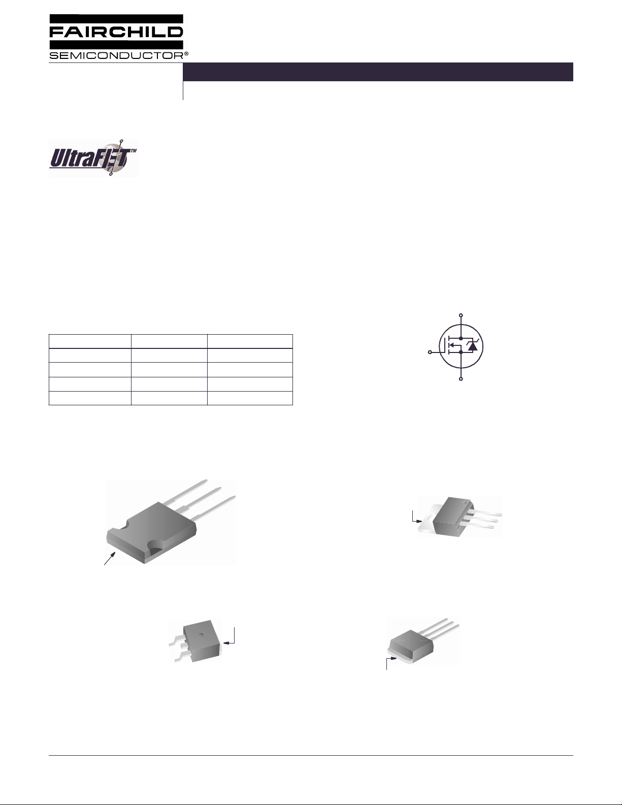
Symbol
D
G
S
Packaging
SOURCE
DRAIN
GATE
DRAIN
(TAB)
TO-247
DRAIN
(FLANGE)
GATE
SOURCE
TO-263AB
This product has been designed to meet the extreme test conditions and environment demanded by the automotive industry. For a copy
of the requirements, see AEC Q101 at: http://www.aecouncil. com/
All Fa irchild semiconductor products are manufactured, assembled a nd tested under ISO9000 and QS9000 qualit y systems certification.
Reliability data can be found at: http:/ /www.mtp.fairchild.com/aut omoti ve.html.
DRAIN
(FLANGE)
DRAIN
(FLANGE)
TO-220AB
SOURCE
TO-262AA
DRAIN
GATE
SOURCE
DRAIN
GATE
©2003 Fairchild Semiconductor Corporation HUFA75344G3, HUFA75344P3, HUFA75344S3S, HUFA75344S3 Rev. B1
HUFA75344G3, HUFA75344P3, HUFA75344S3S
Absolute Maximum Ratings T
= 25oC, Unless Otherwise Specified
C
UNITS
Drain to Source Voltage (Note 1). . . . . . . . . . . . . . . . . . . . . . . . . . . . . . . . . . . . . . . . . . . . . . . V
Drain to Gate Voltage (R
= 20kΩ) (Note 1) . . . . . . . . . . . . . . . . . . . . . . . . . . . . . . . . . . . . . V
GS
Gate to Source Voltage . . . . . . . . . . . . . . . . . . . . . . . . . . . . . . . . . . . . . . . . . . . . . . . . . . . . . . . V
DSS
DGR
GS
55 V
55 V
±20 V
Drain Current
Continuous (Figure 2). . . . . . . . . . . . . . . . . . . . . . . . . . . . . . . . . . . . . . . . . . . . . . . . . . . . . . . . . I
Pulsed Drain Current . . . . . . . . . . . . . . . . . . . . . . . . . . . . . . . . . . . . . . . . . . . . . . . . . . . . . . . .I
Pulsed Avalanche Rating. . . . . . . . . . . . . . . . . . . . . . . . . . . . . . . . . . . . . . . . . . . . . . . . . . . . . . E
Power Dissipation . . . . . . . . . . . . . . . . . . . . . . . . . . . . . . . . . . . . . . . . . . . . . . . . . . . . . . . . . . . . P
Derate Above 25oC . . . . . . . . . . . . . . . . . . . . . . . . . . . . . . . . . . . . . . . . . . . . . . . . . . . . . . . . . . . .
Operating and Storage Temperature . . . . . . . . . . . . . . . . . . . . . . . . . . . . . . . . . . . . . . . . . T
D
DM
AS
D
, T
J
STG
Maximum Temperature for Soldering
Leads at 0.063in (1.6mm) from Case for 10s. . . . . . . . . . . . . . . . . . . . . . . . . . . . . . . . . . . . . . .T
Package Body for 10s, See Techbrief 334 . . . . . . . . . . . . . . . . . . . . . . . . . . . . . . . . . . . . . . . T
CAUTION: Stresses above those listed in “Absolute Maximum Rati ngs” may cause permane nt damage to the device. This is a stress only rating and oper ation of the
device at these or any other conditions above those indicated in the operational sections of this specification is not implied.
L
pkg
75
Figure 4
Figure 6
285
1.90
-55 to 175
300
260
A
W
W/oC
o
C
o
C
o
C
NOTE:
= 25oC to 150oC.
1. T
J
Electrical Specifications T
= 25oC, Unless Otherwise Specified
C
PARAMETER SYMBOL TEST CONDITIONS MIN TYP MAX UNITS
OFF STATE SPECIFICATIONS
Drain t o Source Breakdown Voltage BV
Zero Gat e V ol tag e D rain Curre nt I
Gate to Sour c e Le ak ag e C urr e nt I
DSSID
DSS
GSS
= 250µA, VGS = 0V (Figure 11) 55 - - V
VDS = 50V, VGS = 0V - - 1 µA
= 45V, VGS = 0V, TC = 150oC--250µA
V
DS
VGS = ±20V - - ±100 nA
ON STATE SPECIFICATIONS
Gate to Source Threshold Voltage V
Drain to Source On Resistance r
GS(TH)VGS
DS(ON)ID
= VDS, ID = 250µA (Figure 10) 2 - 4 V
= 75A, VGS = 10V (Figure 9) - 0.006 5 0.008 Ω
THERMAL SPECIFICATIONS
Thermal R esis ta nc e Ju ncti on to Case R
Thermal Resistance Junction to Ambient R
SWITCHING SPECIFICATIONS (V
GS
= 10V)
Turn-On Time t
Turn-On Delay Time t
d(ON)
Rise Time t
Turn-Off Delay Time t
d(OFF)
Fall Time t
Turn-Off Time t
θJC
θJA
ON
r
f
OFF
(Figure 3) - - 0.52
TO-247 - - 30
TO-220, TO-263, TO-262 - - 62
VDD = 30V, ID ≅ 75A,
R
= 0.4Ω, VGS = 10V,
L
R
= 3.0Ω
GS
--195ns
-16- ns
-112- ns
-37- ns
-28- ns
--100ns
o
C/W
o
C/W
o
C/W
GATE CHARGE SPECIFICATIONS
Total Gate Charg e Q
g(TOT)VGS
Gate Charge at 10V Q
Threshold Gat e Ch arg e Q
Gate to Source Gate Charg e Q
Reverse Transfer Capacitance Q
g(10)
g(TH)
gs
gd
= 0V to 20V VDD = 30V,
I
≅ 75A,
VGS = 0V to 10V - 9 0 10 8 nC
VGS = 0V to 2V - 5.9 7.0 nC
D
R
= 0.4Ω
L
I
g(REF)
= 1.0mA
(Figure 13)
-175210nC
-14-nC
-39-nC
CAPACITANCE SPECIFICATIONS
Input Capacitance C
Output Capacitance C
Reverse Transfer Capacitance C
ISS
OSS
RSS
VDS = 25V, VGS = 0V,
f = 1MHz
(Figure 12)
-3200- pF
-1170- pF
-310- pF
©2003 Fairchild Semiconductor Corporation HUFA75344G3, HUFA75344P3, HUFA75344S3S, HUFA75344S3 Rev. B1
HUFA75344G3, HUFA75344P3, HUFA75344S3S
Source to Drain Diode Specifications
PARAMETER SYMBOL TEST CONDITIONS MIN TYP MAX UNITS
Source to Drain Diode Vol tage V
Reverse Recovery Time t
Reverse Recovered Charge Q
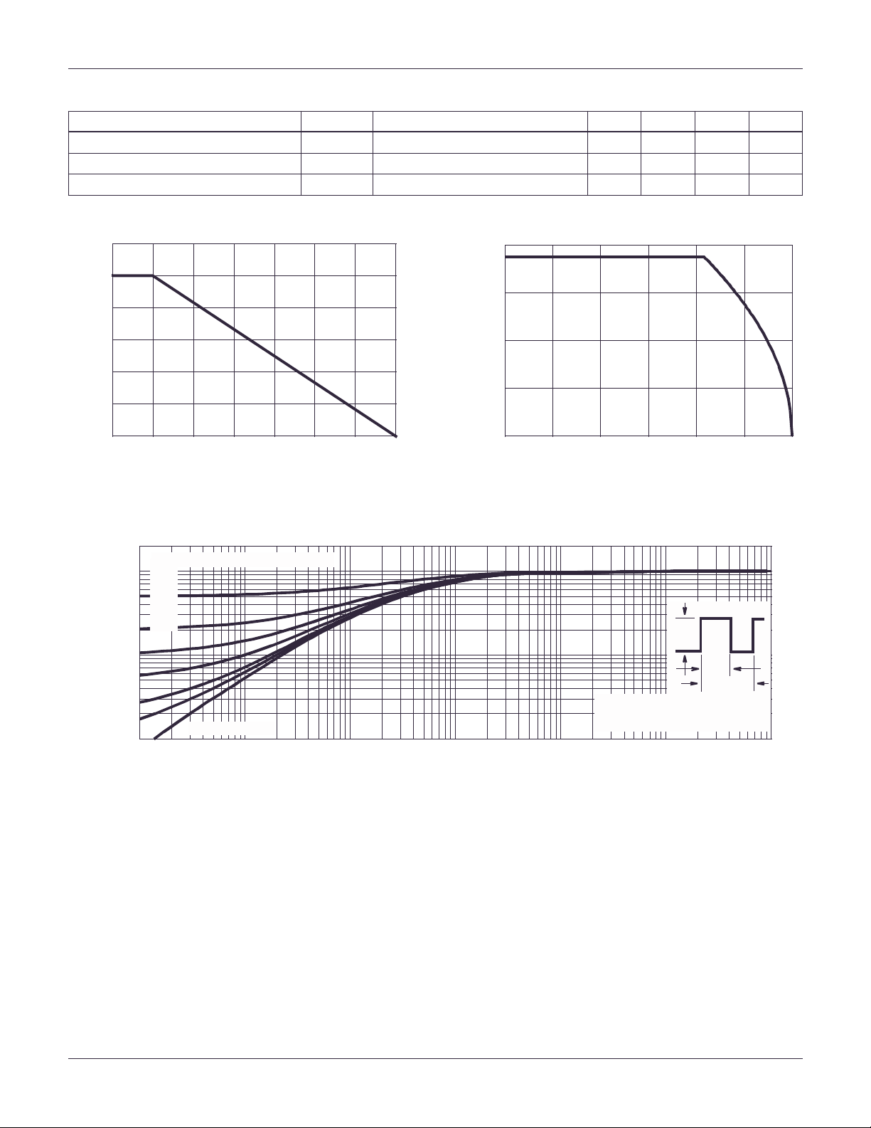
Typical Performance Curves
1.2
1.0
0.8
SD
rr
RR
ISD = 75A - - 1.25 V
ISD = 75A, dISD/dt = 100A/µs--105ns
ISD = 75A, dISD/dt = 100A/µs - - 210 nC
80
60
0.6
0.4
0.2
POWER DISSIPATION MULTIPLIER
0
0 25 50 75 100 150
TC, CASE TEMPERATURE (oC)
125 175
FIGURE 1. NORMALIZED POWER DISSIPATION vs CASE
TEMPERATURE
2
DUTY CYCLE - DESCENDING ORDER
0.5
1
0.2
0.1
0.05
0.02
0.01
0.1
, NORMALIZED
θJC
Z
THERMAL IMPEDANCE
0.01
-5
10
SINGLE PULSE
-4
10
-3
10
t, RECTANGULAR PULSE DURATION (s)
FIGURE 3. NORMALIZED MAXIMUM TRANSIENT THERMAL IMPEDANCE
40
20
, DRAIN CURRENT (A)
D
I
0
25
50 75 100 125 150 175
TC, CASE TEMPERATURE (oC)
FIGURE 2. MAXIMUM CONTINUOUS DRAIN CURRENT vs
CASE TEMPERATURE
P
DM
t
1
NOTES:
DUTY FACTOR: D = t
PEAK TJ = PDM x Z
-2
10
-1
10
1/t2
x R
θJC
θJC
0
10
t
2
+ T
C
1
10
©2003 Fairchild Semiconductor Corporation HUFA75344G3, HUFA75344P3, HUFA75344S3S, HUFA75344S3 Rev. B1
 Loading...