

Fairchild Semiconductor HUF75639S3 Datasheet
Data Sheet December 2001
56A, 115V, 0.025 Ohm, N-Channel
UltraFET Power MOSFET
This N-Channel power MOSFETs is manufactured using the
innovative UltraFET® process. This advanced process
technology achieves the lowest possible on-resistance per
silicon area, resul ting in outstanding performance. This
device is capable of withstanding high energy in the
avala nc he mod e and the dio de exhibits very low rev erse
recovery time and stored charge. It was designed for use in
applications where power efficiency is important, such as
switching regu la tors, switching converters, motor drivers,
relay drivers, low-voltage bus switches, and power
management in portable and battery-operated products.
Formerly developmental type TA75639.‘
Ordering Information
PART NUMBER PACKAGE BRAND
HUF75639S3R4851 TO-262AA R4851
NOTE: When ordering, use the entire part number.
Symbol
D
G
HUF75639S3R4851
Features
• 56A, 115V
• Simulation Models
- Temperature Compensated PSPICE® and SABER™
Electrical Models
- Spice and Saber Thermal Impedance M ode ls
- www.fairchildsemi.com
• Peak Current vs Pulse Width Curve
• UIS Rating Curve
• Related Literature
- TB334, “Guidelines for Soldering Surface Mount
Components to PC Boards”
Packaging
JEDEC TO-262AA
SOURCE
DRAIN
GATE
Absolute Maximum Ratings
Drain to Source Voltage (Note 1) . . . . . . . . . . . . . . . . . . . . . . . . . . . . . . . . . . . . . . . . . . . . . . . V
Drain to Gate Voltage (R
Gate to Source Voltage . . . . . . . . . . . . . . . . . . . . . . . . . . . . . . . . . . . . . . . . . . . . . . . . . . . . . . . V
Drain Current
Continuous (Figure 2). . . . . . . . . . . . . . . . . . . . . . . . . . . . . . . . . . . . . . . . . . . . . . . . . . . . . . . . . I
Pulsed Drain Current . . . . . . . . . . . . . . . . . . . . . . . . . . . . . . . . . . . . . . . . . . . . . . . . . . . . . . . . I
Pulsed Avalanche Rating. . . . . . . . . . . . . . . . . . . . . . . . . . . . . . . . . . . . . . . . . . . . . . . . . . . . . . E
Power Dissipation . . . . . . . . . . . . . . . . . . . . . . . . . . . . . . . . . . . . . . . . . . . . . . . . . . . . . . . . . . . . P
Derate Above 25oC . . . . . . . . . . . . . . . . . . . . . . . . . . . . . . . . . . . . . . . . . . . . . . . . . . . . . . . . . . . .
Operating and Storage Temperature . . . . . . . . . . . . . . . . . . . . . . . . . . . . . . . . . . . . . . . . . T
Maximum Temperature for Soldering
Leads at 0.063in (1.6mm) from Case for 10s. . . . . . . . . . . . . . . . . . . . . . . . . . . . . . . . . . . . . . . T
Package Body for 10s, See Techbrief 334 . . . . . . . . . . . . . . . . . . . . . . . . . . . . . . . . . . . . . . . T
CAUTION: Stresses above those listed in “A bsolute Maximu m Rating s” may cause per manent d amage to t he device. This is a str ess on ly rating and operation o f the
device at these or any other conditions above those indicated in the operational sections of this specification is not implied.
NOTE:
= 25oC to 150oC.
1. T
J
Product reliability information can be found at http://www.fairchildsemi.com/products/discrete/reliability/index.html
All Fairchild semiconductor products are manufactured, assembled and tested under ISO9000 and QS9000 quality systems certification.
GS
S
TC = 25oC, Unless Otherwise Specified
= 20kΩ) (Note 1) . . . . . . . . . . . . . . . . . . . . . . . . . . . . . . . . . . . . . V
, T
J
For severe environments, see our Automotive HUFA series.
DSS
DGR
GS
DM
AS
STG
pkg
HUF75639S3R4851 UNITS
115 V
115 V
±20 V
D
D
L
56
Figure 4
Figures 6, 14, 15
200
1.35
-55 to 175
300
260
A
W
W/oC
o
C
o
C
o
C
©2001 Fairchild Semiconductor Corpo ration HUF75639S3R4851 Rev. B
HUF75639S3R4851
Electrical Specifications
TC = 25oC, Unless Otherwise Specified
PARAMETER SYMBOL TEST CONDITIONS MIN TYP MAX UNITS
OFF STATE SPECIFICATIONS
Drain to Source Breakdown Voltage BV
Zero Gate Voltage Drain Current I
Gate to Source Leakage Current I
ON STATE SPECIFICATIONS
Gate to Source Threshold Voltage V
Drain to Source On Resistance r
THERMAL SPECIFICATIONS
Thermal Resistance Junction to Case R
Thermal Resistance Junction to Ambient R
SWITCHING SPECIFICATIONS (V
GS
= 10V)
Turn-On Time t
Turn-On Delay Time t
Rise Time t
Turn-Off Delay Time t
Fall Time t
Turn-Off Time t
GATE CHARGE SPECIFICATIONS
DSSID
DSS
VDS = 95V, VGS = 0V - - 1 µA
V
GSS
GS(TH)VGS
DS(ON)ID
θJC
θJA
ON
VGS = ±20V - - ±100 nA
(Figure 3) - - 0.74
TO-262 - - 62
VDD = 50V, ID ≅ 56A,
R
d(ON)
d(OFF)
OFF
R
r
f
= 250µA, VGS = 0V (Figure 11) 115 - - V
= 90V, VGS = 0V, TC = 150oC--250µA
DS
= VDS, ID = 250µA (Figure 10) 2 - 4 V
= 56A, VGS = 10V (Figure 9) - 0.021 0.025 Ω
o
o
--110ns
= 0.89Ω, VGS = 10V,
L
GS
= 5.1Ω
-15- ns
-60- ns
-20- ns
-25- ns
- - 70 ns
C/W
C/W
Total Gate Charge Q
Gate Charge at 10V Q
Threshold Gate Charge Q
Gate to Source Gate Charge Q
Reverse Transfer Capacitance Q
CAPACITANCE SPECIFICATIONS
Input Capacitance C
Output Capacitance C
Reverse Transfer Capacitance C
Source to Drain Diode Specifications
PARAMETER SYMBOL TEST CONDITIONS MIN TYP MAX UNITS
Source to Drain Diode Voltage V
Reverse Recovery Time t
Reverse Recovered Charge Q
g(TOT)VGS
g(10)
g(TH)
ISS
VGS = 0V to 10V - 57 75 nC
VGS = 0V to 2V - 3.7 4.5 nC
gs
gd
VDS = 25V, VGS = 0V,
f = 1MHz
SD
rr
RR
(Figure 12)
ISD = 56A - - 1.25 V
ISD = 56A, dISD/dt = 100A/µs - - 110 ns
ISD = 56A, dISD/dt = 100A/µs - - 320 nC
OSS
RSS
= 0V to 20V VDD = 50V,
I
≅ 56A,
D
= 0.89Ω
R
L
I
= 1.0mA
g(REF)
(Figure 13)
- 110 130 nC
-9.8- nC
-24-nC
- 2000 - pF
- 500 - pF
-65-pF
©2001 Fairchild Semiconductor Corpo ration HUF75639S3R4851 Rev. B
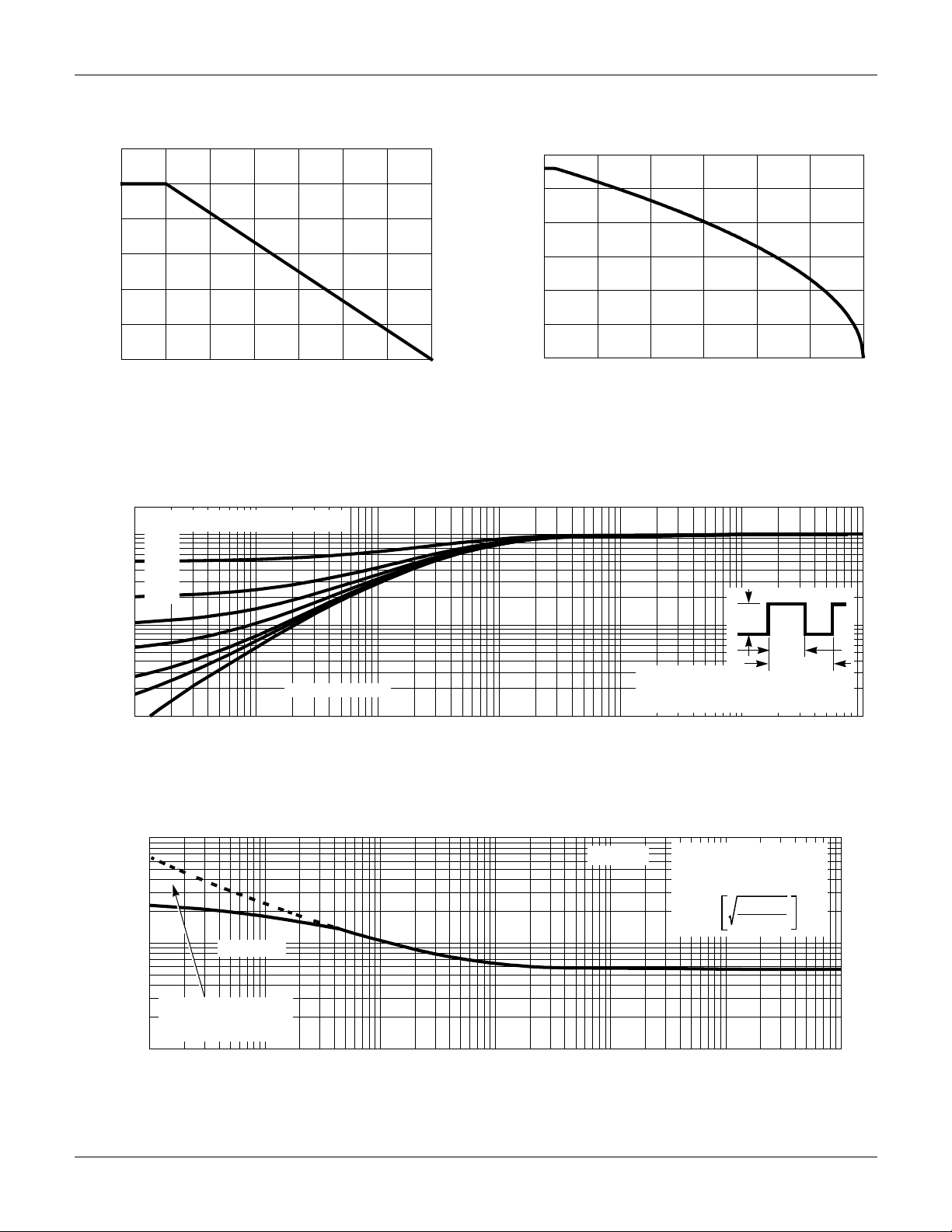
Typical Performance Curves
1
HUF75639S3R4851
1.2
1.0
0.8
0.6
0.4
0.2
POWER DISSIPATION MULTIPLIER
0
0 25 50 75 100 150
125 175
TC, CASE TEMPERATURE (oC)
FIGURE 1. NORMALIZED POWER DISSIP ATION vs CASE
TEMPERATURE
2
DUTY CYCLE - DESCENDING ORDER
1
0.5
0.2
0.1
0.05
0.02
0.01
0.1
, NORMALIZED
θJC
Z
THERMAL IMPEDANCE
SINGLE PULSE
0.01
-5
10
-4
10
-3
10
t, RECTANGULAR PULSE DURATION (s)
60
50
40
30
20
, DRAIN CURRENT (A)
D
I
10
0
25 50 75 100 125 150 175
T
, CASE TEMPERATURE (oC)
C
FIGURE 2. MAXIMUM CONTINUOUS DRAIN CURRENT vs
CASE TEMPERATURE
P
DM
NOTES:
DUTY FACTOR: D = t
PEAK TJ = PDM x Z
-2
10
-1
10
10
θJC
1/t2
0
x R
θJC
t
1
t
2
+ T
C
10
FIGURE 3. NORMALIZED MAXIMUM TRANSIENT THERMAL IMPEDANCE
, PEAK CURRENT (A)
I
DM
1000
100
TRANSCONDUCTANCE
MAY LIMIT CURRENT
IN THIS REGION
10
-5
10
VGS = 10V
10
TC = 25oC
-4
-3
10
-2
10
-1
10
t, PULSE WIDTH (s)
FOR TEMPERATURES
ABOVE 25
o
C DERATE PEAK
CURRENT AS FOLLOWS:
175 - T
I = I
25
0
10
C
150
1
10
FIGURE 4. PEAK CURRENT CAPAB ILITY
©2001 Fairchild Semiconductor Corpo ration HUF75639S3R4851 Rev. B
 Loading...