

Fairchild Semiconductor HUF75631S3S Datasheet
©2001 Fairchild Semiconductor Corpo ration HUF75631P3, HUF75631S3ST Rev. B
HUF75631P3, HUF75631S3ST
33A, 100V, 0.040 Ohm, N-Channel,
UltraFET® Power MOSFETs
Packaging
Symbol
Features
• Ultra Low On-Resistance
-r
DS(ON)
= 0.040Ω, V
GS
= 10V
• Simulation Models
- Temperature Compensated PSPICE® and SABER™
Electrical Models
- Spice and SABER Thermal Impedance Models
- www.fairchildsemi.com
• Peak Current vs Pulse Width Curve
• UIS Rating Curve
Product reliability information can be found at http://www.fairchildsemi.com/products/discrete/reliability/index.html
For severe environments, see our Automotive HUFA series.
All Fairchild semiconductor products are manufactured, assembled and tested under ISO9000 and QS9000 quality systems certification.
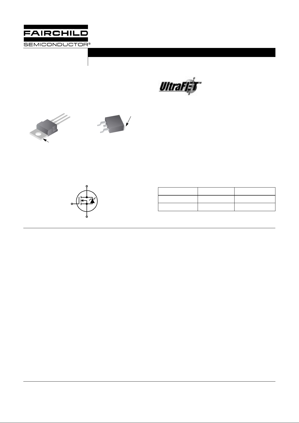
DRAIN
(FLANGE)
DRAIN
SOURCE
GATE
HUF75631P3
JEDEC TO-220AB JEDEC TO-263AB
HUF75631S3ST
GATE
SOURCE
DRAIN
(FLANGE)
D
G
S
Ordering Information
PART NUMBER PACKAGE BRAND
HUF75631P3 TO-220AB 75631P
HUF75631S3ST TO-263AB 75631S
NOTE: When ordering, use the entire part number, e.g.,
HUF75631S3ST.
Absolute Maximum Ratings
TC = 25oC, Unless Otherwise Specified
HUF75631P3
HUF75631S3ST UNITS
Drain to Source Voltage (Note 1) . . . . . . . . . . . . . . . . . . . . . . . . . . . . . . . . . . . . . . . . . . . . . V
DSS
100 V
Drain to Gate Voltage (R
GS
= 20kΩ) (Note 1) . . . . . . . . . . . . . . . . . . . . . . . . . . . . . . . . . . .V
DGR
100 V
Gate to Source Voltage . . . . . . . . . . . . . . . . . . . . . . . . . . . . . . . . . . . . . . . . . . . . . . . . . . . . .V
GS
±20 V
Drain Current
Continuous (T
C
= 25oC, VGS = 10V) (Figure 2) . . . . . . . . . . . . . . . . . . . . . . . . . . . . . . . . I
D
Continuous (TC = 100oC, VGS = 10V) (Figure 2) . . . . . . . . . . . . . . . . . . . . . . . . . . . . . . . I
D
Pulsed Drain Current . . . . . . . . . . . . . . . . . . . . . . . . . . . . . . . . . . . . . . . . . . . . . . . . . . . . . I
DM
33
23
Figure 4
A
A
Pulsed Avalanche Rating . . . . . . . . . . . . . . . . . . . . . . . . . . . . . . . . . . . . . . . . . . . . . . . . . . . UIS Figures 6, 14, 15
Power Dissipation 8 . . . . . . . . . . . . . . . . . . . . . . . . . . . . . . . . . . . . . . . . . . . . . . . . . . . . . . . . . P
D
Derate Above 25oC . . . . . . . . . . . . . . . . . . . . . . . . . . . . . . . . . . . . . . . . . . . . . . . . . . . . . . . . .
120
0.80
W
W/oC
Operating and Storage Temperature . . . . . . . . . . . . . . . . . . . . . . . . . . . . . . . . . . . . . . . T
J
, T
STG
-55 to 175
o
C
Maximum Temperature for Soldering
Leads at 0.063in (1.6mm) from Case for 10s. . . . . . . . . . . . . . . . . . . . . . . . . . . . . . . . . . . . T
L
Package Body for 10s, See Techbrief TB334. . . . . . . . . . . . . . . . . . . . . . . . . . . . . . . . . . . T
pkg
300
260
o
C
o
C
NOTE:
1. T
J
= 25oC to 150oC.
CAUTION: Stresses above those listed in “ Absolute M aximum Ratings” may cause perm anent damage to th e device. This is a stress onl y rating and operation of the
device at these or any other conditions above those indicated in the operational sections of this specification is not implied.
Data Sheet December 2001
©2001 Fairchild Semiconductor Corporati on HUF75631P3, HUF75631S3ST Rev. B
Electrical Specifications
TC = 25oC, Unless Otherwise Specified
PARAMETER SYMBOL TEST CONDITIONS MIN TYP MAX UNITS
OFF STATE SPECIFICATIONS
Drain to Source Breakdown Voltage BV
DSSID
= 250µA, VGS = 0V (Figure 11) 100 - - V
Zero Gate Voltage Drain Current I
DSS
VDS = 95V, VGS = 0V - - 1 µA
V
DS
= 90V, VGS = 0V, TC = 150oC - - 250 µA
Gate to Source Leakage Current I
GSS
VGS = ±20V - - ±100 nA
ON STATE SPECIFICATIONS
Gate to Source Threshold Voltage V
GS(TH)VGS
= VDS, ID = 250µA (Figure 10) 2 - 4 V
Drain to Source On Resistance r
DS(ON)ID
= 33A, VGS = 10V (Figure 9) - 0.033 0.040 Ω
THERMAL SPECIFICATIONS
Thermal Resistance Junction to Case R
θJC
TO-220, TO-263 - - 1.25oC/W
Thermal Resistance Junction to
Ambient
R
θJA
--62oC/W
SWITCHING SPECIFICATIONS (V
GS
= 10V)
Turn-On Time t
ON
VDD = 50V, ID = 33A
V
GS
= 10V,
R
GS
= 9.1Ω
(Figures 18, 19)
- - 100 ns
Turn-On Delay Time t
d(ON)
-9.5-ns
Rise Time t
r
-57-ns
Turn-Off Delay Time t
d(OFF)
-40-ns
Fall Time t
f
- 55 - ns
Turn-Off Time t
OFF
- - 145 ns
GATE CHARGE SPECIFICATIONS
Total Gate Charge Q
g(TOT)VGS
= 0V to 20V VDD = 50V,
I
D
= 33A,
I
g(REF)
= 1.0mA
(Figures 13, 16, 17)
-6679nC
Gate Charge at 10V Q
g(10)
VGS = 0V to 10V - 35 42 nC
Threshold Gate Charge Q
g(TH)
VGS = 0V to 2V - 2.4 2.9 nC
Gate to Source Gate Charge Q
gs
-5.4-nC
Gate to Drain “Miller” Charge Q
gd
-13-nC
CAPACITANCE SPECIFICATIONS
Input Capacitance C
ISS
VDS = 25V, VGS = 0V,
f = 1MHz
(Figure 12)
- 1220 - pF
Output Capacitance C
OSS
- 295 - pF
Reverse Transfer Capacitance C
RSS
- 100 - pF
Source to Drain Diode Specifications
PARAMETER SYMBOL TEST CONDITIONS M IN TYP MAX UNITS
Source to Drain Diode Voltage V
SD
ISD = 33A - - 1.25 V
I
SD
= 17A - - 1.00 V
Reverse Recovery Time t
rr
ISD = 33A, dISD/dt = 100A/µs - - 112 ns
Reverse Recovered Charge Q
RR
ISD = 33A, dISD/dt = 100A/µs - - 400 nC
HUF75631P3, HUF75631S3ST
©2001 Fairchild Semiconductor Corporati on HUF75631P3, HUF75631S3ST Rev. B
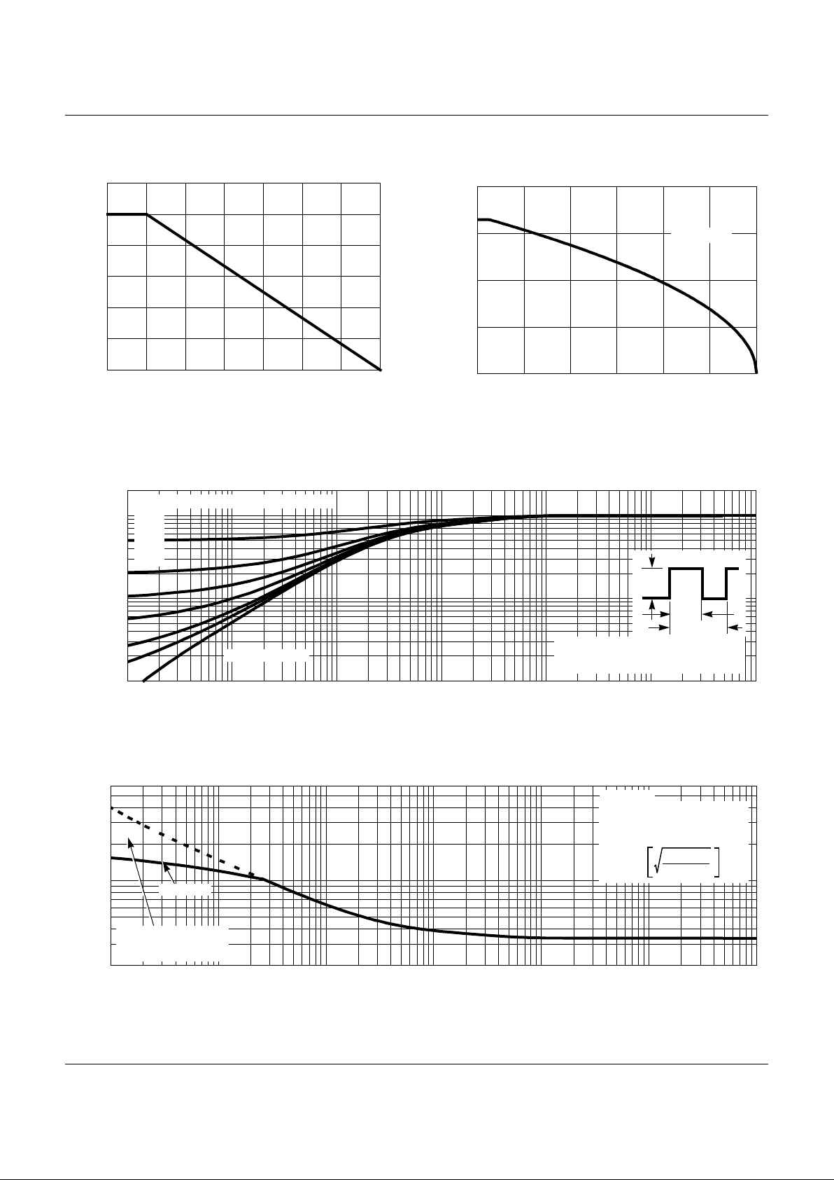
Typical Performance Curves
FIGURE 1. NORMALIZED POWER DISSIP A TI ON vs CASE
TEMPERATURE
FIGURE 2. MAXIMUM CONTINUOUS DRAIN CURRENT vs
CASE TEMPERATURE
FIGURE 3. NORMALIZED MAXIMUM TRANSIENT THERMAL IMPEDANCE
FIGURE 4. PEAK CURRENT CAPA BILITY
TC, CASE TEMPERATURE (oC)
POWER DISSIPATION MULTIPLIER
0
0 25 50 75 100 17
5
0.2
0.4
0.6
0.8
1.0
1.2
125
150
20
30
40
50 75 100 125 150
0
25
I
D
, DRAIN CURRENT (A)
TC, CASE TEMPERATURE (oC)
V
GS
= 10V
17
5
10
0.1
1
2
10
-4
10
-3
10
-2
10
-1
10
0
10
1
0.01
10
-5
t, RECTANGULAR PULSE DURATION (s)
Z
θJC
, NORMALIZED
THERMAL IMPEDANCE
SINGLE PULSE
NOTES:
DUTY FACTOR: D = t
1/t2
PEAK TJ = PDM x Z
θJC
x R
θJC
+ T
C
P
DM
t
1
t
2
DUTY CYCLE - DESCENDING ORDER
0.5
0.2
0.1
0.05
0.01
0.02
100
600
20
10
-4
10
-3
10
-2
10
-1
10
0
10
1
10
-5
I
DM
, PEAK CURRENT (A)
t, PULSE WIDTH (s)
TRANSCONDUCTANCE
MAY LIMIT CURRENT
IN THIS REGION
TC = 25oC
I = I
25
175 - T
C
150
FOR TEMPERATURES
ABOVE 25
o
C DERATE PEAK
CURRENT AS FOLLOWS:
VGS = 10V
HUF75631P3, HUF75631S3ST
 Loading...