

Fairchild Semiconductor FSTUD32450 Datasheet
August 2001
Revised July 2002
FSTUD32450
Configurable 4-Bit to 40-Bit Bus Switch with
−2V Undershoot Protection and Selectable Level Shifting
FSTUD32450 Configurable 4-Bit to 40-Bit Bus Switch with
Shifting
General Description
The Fairchild Universal Bus Switch FSTUD32450 provides
4-bit, 5-bit, 8-bit, 10 -bit, 16 -bit, 2 0-bit...4 0-bit o f high- speed
CMOS TTL-compatible bus switching. The low On Re sistance of the switch allows inputs to be connect ed to outputs without adding propagation delay or generating
additional ground bounce noise.
The FSTUD32450 is designed to allow “customer” configuration control of the enable connections. The device can be
organized as eithe r a ten 4-bit, eight 5-bit , four 10-bit, two
20-bit or one 40-bit enable d bus switch. Also achievable
are 8-bit and 16-bit enab led co nfigura tion s (see Fu nctional
Description). The device's bit configuration is controlled
through select pin logic. (s ee Truth Table). When OE
LOW, Port A
the switch is OPEN.
The A and B Ports are protected against undershoot to
support an extended range to 2.0V below ground.
Fairchild's integrated Undershoot Hardened Circuit
( UHC
preventing voltage differentials from developing and turning the switch on.
Another innovative devi ce featur e is the ad dition of a level
shifting select pin, “S
the device behaves as a standard N-MOS switch. When S
and S5 are HIGH, a diode to VCC is integrated into the circuit allowing for level sh ifting between 5V inputs and 3.3V
outputs.
is connected to Port Bx. When OEx is HIGH,
x
) senses undershoot at the I/O, and responds by
and S5”. When S2 and S5 are LOW,
2
Features
■ Undershoot protected to −2V (A and B Ports)
■ Voltage level shifting
■ 4
Ω switch connection between two ports
■ Minimal propagation delay through the switch
■ Low l
CC
■ Zero bounce in flow-through mode
■ Control inputs compatible with TTL level
■ See Applications Notes AN -5008 and AN -5021 for UHC
details
■ Packaged in plastic Fine-Pitch Ball Grid Array (FBGA)
is
x
Applications Note
Select pins S0, S1, S2, S3, S4 and S5 are intended to be
used as static user confi gurable control pins. The AC p er-
formance of these pins has not been characterized or
tested. Switching of these select pins during system operation may temporarily disrupt output logic states and/or
enable pin controls.
40-bit configuration can be achieved by connecting the
OE
and the OE6 pins to together.
1
2
Ordering Code:
Order Number Package Number Package Description
FSTUD32450G
(Note 1)(Note 2)
Note 1: Ordering code “G” indicates Trays.
Note 2: Devices also available in Tape and Reel. Specify by appending th e s uffix let t er “X” to the ordering code.
BGA114A 114-Ball Fine-Pitch Ball Grid Array (FBGA), JEDEC MO-205, 5.5mm Wide
−
2V Undershoot Protection and Selectable Level
UHC is a trademark of Fairchild Semiconductor Corporation.
© 2002 Fairchild Semiconductor Corporation DS500447 www.fairchildsemi.com
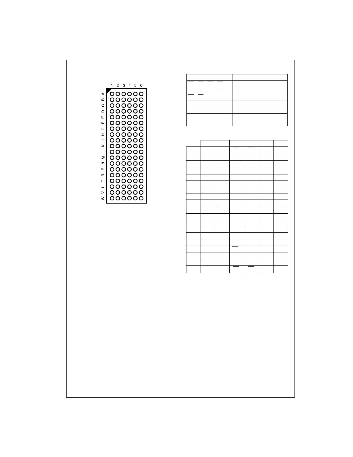
Connection Diagram
Pin Assignment for FBGA
FSTUD32450
(Top Thru View)
Pin Descriptions
Pin Name Description
OE
, OE2, OE3, OE4, Bus Switch
1
, OE6, OE7, OE8Enables
OE
5
OE
, OE
9
10
1A, 2A, 3A, 4A Bus A
1B, 2B, 3B, 4B Bus B
, S1, S3, S
S
0
S
, S
2
4
5
Bit Configuration Enables
Level Shifting Diode Enables
FBGA Pin Assignments
123456
A 1A
B 1A61A51A11B11B51B
C 1A81A71A31B31B71B
D 1A101A9GND OE51B91B
E 2A22A1S0V
F 2A42A3S
G 2A62A5VCCGND 2B52B
H 2A82A7GND GND 2B72B
J 2A102A9GND GND 2B92B
K OE4OE8GND GND OE9OE
L 3A103A9GND GND 3B93B
M 3A83A7GND GND 3B73B
N 3A63A5GND V
P 3A43A3S
R 3A23A1V
T 4A104A9OE10GND 4B94B
U 4A84A74A34B34B74B
V 4A64A54A14B14B54B
W 4A44A2OE7OE64B24B
1A2OE1OE21B21B
4
CC
S22B32B
1
CC
S43B33B
5
S33B13B
CC
2B12B
3B53B
4
6
8
10
2
4
6
8
10
3
10
8
6
4
2
10
8
6
4
www.fairchildsemi.com 2
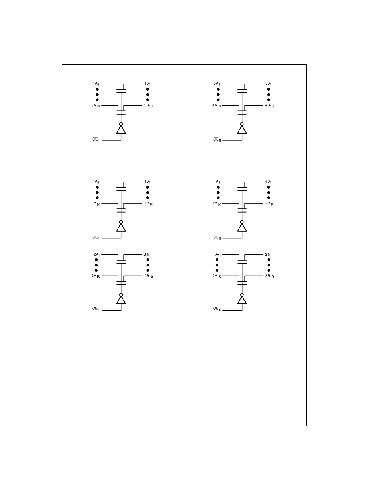
Logic Diagrams
FSTUD32450
20-Bit Configuration
10-Bit Configuration
3 www.fairchildsemi.com
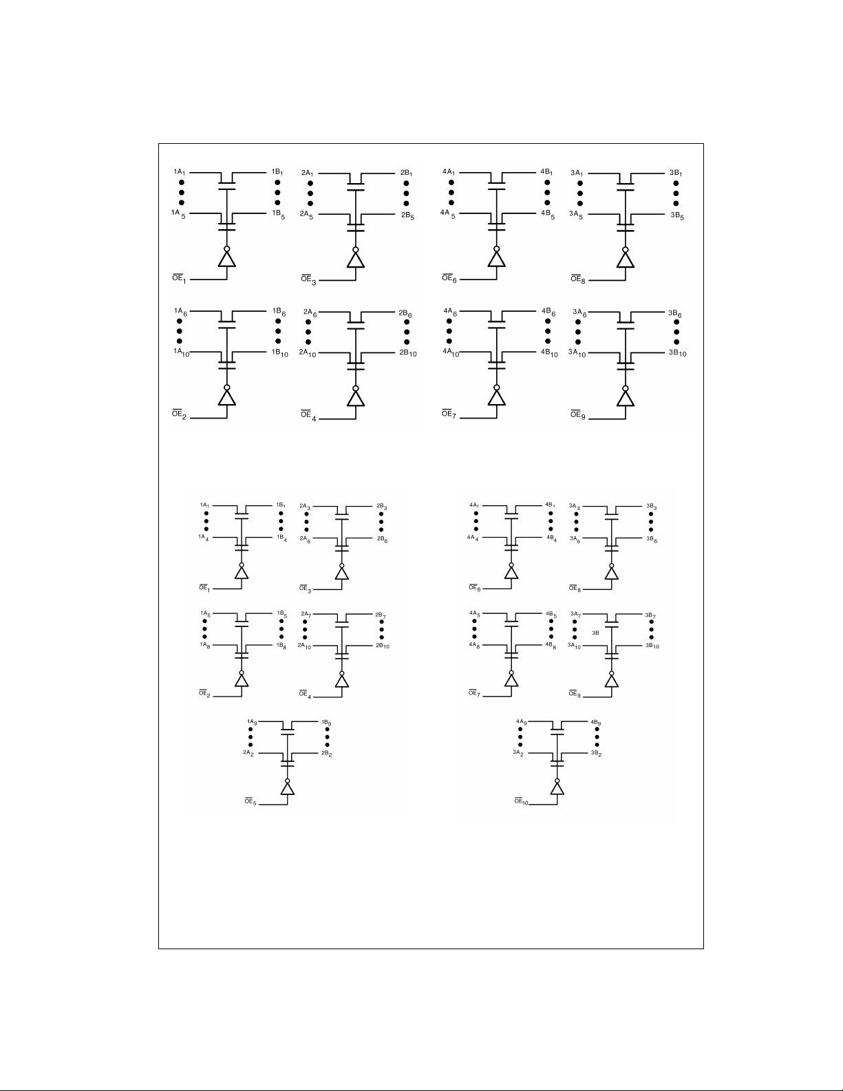
FSTUD32450
5-Bit Configuration
4-Bit Configuration
www.fairchildsemi.com 4
 Loading...