

Fairchild Semiconductor FSTUD162450 Datasheet
April 2001
Revised August 2001
FSTUD162450
Configurable 4-Bit to 20-Bit Bus Switch with
−2V Undershoot Protection and Selectable Level Shifting
and 25Ω Series Resistors in Outputs
FSTUD162450 Configurable 4-Bit to 20-Bit Bus Switch with
Shifting and 25
Ω
Series Resistors in Outputs
General Description
The Fairchild Universal Bus Switch FSTUD162450 provides 4-bit, 5-bit, 8-bit, 10-bit, 16-bit, 20-bit of high-speed
CMOS TTL-compatible bus switching. The low On Re sistance of the switch allows inputs to be connect ed to outputs without adding propagation delay or generating
additional ground bounce noise.
The FSTUD162450 is desi gne d to all ow “cu s tom er ” conf iguration control of the enable connections. The device can
be organized as either a five 4-bit, four 5-bi t, two 10-bit or
one 20-bit bus switc h. Also available are 8-b it and 16-bit
enabled configur ations (see Functional Description). The
device's bit configur ation is controlled through select pin
logic. (see Truth Table). When OE
nected to Port B
The A and B Ports are protected against undershoot to
support an extended range to 2.0V below ground.
Fairchild's integrated Undershoot Hardened Circuit
(UHC
) senses undershoot at the I/O and responds by
preventing voltage differentials from developing and turning the switch on.
Another innovative devi ce featur e is the ad dition of a level
shifting select pin, “S
behaves as a standard N-MOS switch. When S
diode to V
shifting between 5V inputs and 3.3V outputs.
. When OEx is HIGH, the switch is OPEN.
x
”. When S2 is LOW, the device
2
is integrated into the circuit allowing for level
CC
is LOW, Port Ax is con-
x
is HIGH, a
2
Features
■ Undershoot protected to −2V (A and B Ports)
■ Voltage level shifting
■ 25
Ω switch connection between two ports
■ Minimal propagation delay through the switch
■ Low l
CC
■ Zero bounce in flow-through mode
■ Control inputs compatible with TTL level
■ See Applications Notes AN-5008 and AN-5021
for UHC details
■ Also packaged in plastic Fine-Pitch Ball Grid Array
(FBGA) (Preliminary)
Applications Note
Select pins S0, S1, S2 are intended to be used as static
user configurable control pins. The AC performance of
these pins has not be en characterized or teste d. Swit ching
of these select pin s during system operation may temporarily disrupt output logic states and/or enable pin controls.
Ordering Code:
Order Number Package Number Package Description
FSTUD162450GX
(Note 1)
FSTUD162450MTD MTD56 56-Lead Thin Shrink Small Outline Package (TSSOP), JEDEC MO-153, 6.1mm Wide
Devices also availab l e in Tape and Reel. Specify by appending th e s uffix let t er “X” to the ordering code.
Note 1: BGA package available in Tape and Reel only.
BGA54A
Preliminary
54-Ball Fine-Pitch Ball Grid Array (FBGA), JEDEC MO-205, 5.5mm Wide
[Tape and Reel]
−
2V Undershoot Protection and Selectable Level
UHC is a trademark of Fairchild Semiconductor Corporation.
© 2001 Fairchild Semiconductor Corporation DS500469 www.fairchildsemi.com
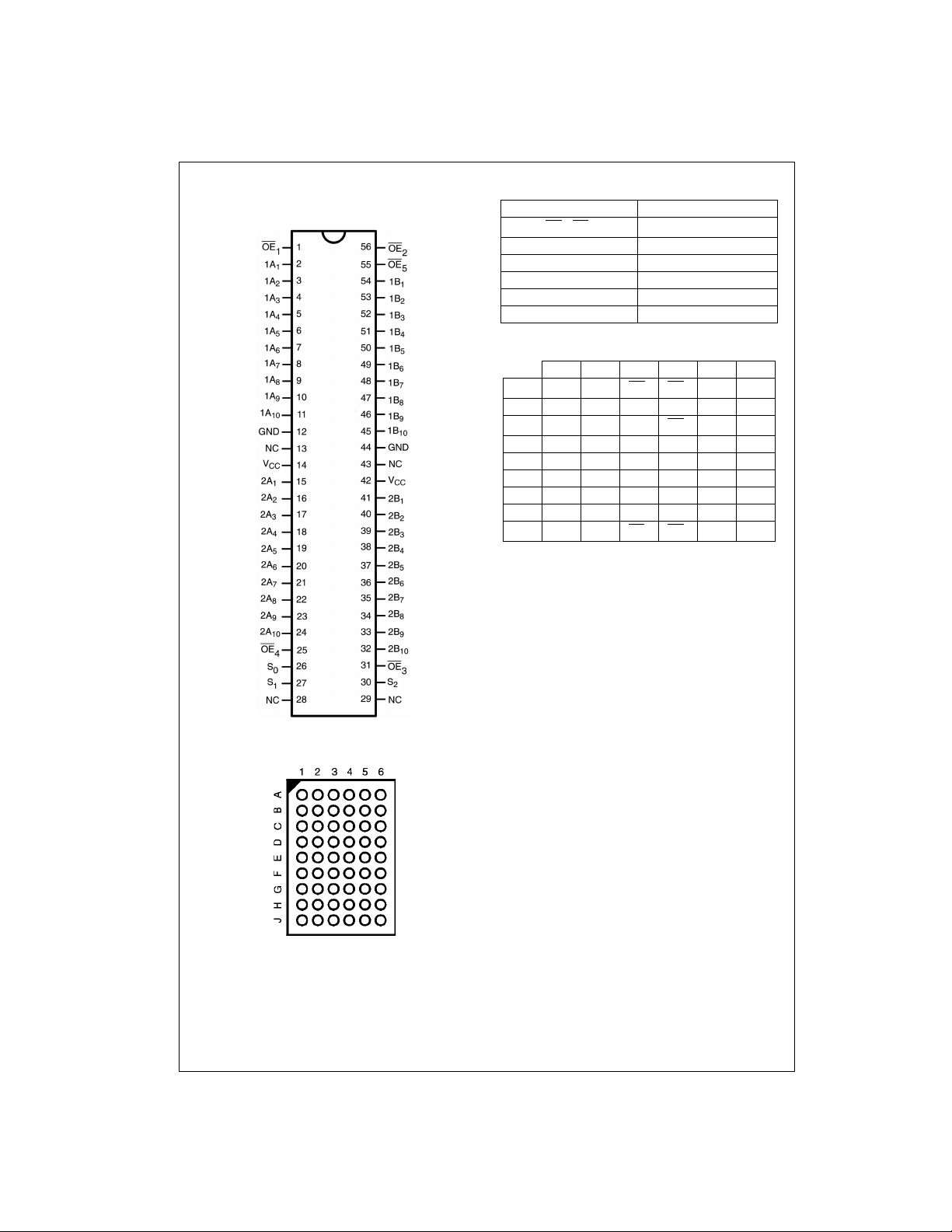
Connection Diagrams
Pin Assignment for TSSOP
FSTUD162450
Pin Descriptions
Pin Name Description
OE
, OE
1
2
Bus Switch Enables
1A, 2A Bus A
1B, 2B Bus B
S
, S
0
1
S
2
Bit Configuration Enables
Level Shifting Diode Enable
NC No Connect
FBGA Pin Assignments
123456
A 1A
B 1A51A41A11B11B41B
C 1A71A6GND OE51B61B
D 1A91A8GND V
E 2A11A
F 2A32A2S
G 2A52A4VCCGND 2B42B
H 2A72A62A102B102B62B
J 2A92A8OE4OE32B82B
1A2OE1OE21B21B
3
CC
10S0VCC1B10
S22B22B
1
1B81B
2B
3
5
7
9
1
3
5
7
9
Pin Assignment for FBGA
(Top Thru View)
www.fairchildsemi.com 2
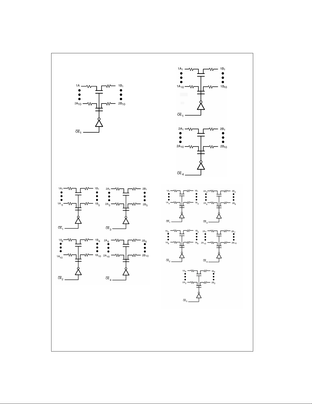
Logic Diagrams
20-Bit Configuration
FSTUD162450
10-Bit Configuration
5-Bit Configuration
4-Bit Configuration
3 www.fairchildsemi.com
Functional Description
The device can also be configured as an 8 and 16-bit device by grounding the unused pins in the 10-bit and 20-bit configurations respectively. The 8-bit configuration may also be achieved by connecting two of the 4-bit enables from the 4-bit configuration together and connecting the remaining enable pin (OE
) HIGH.
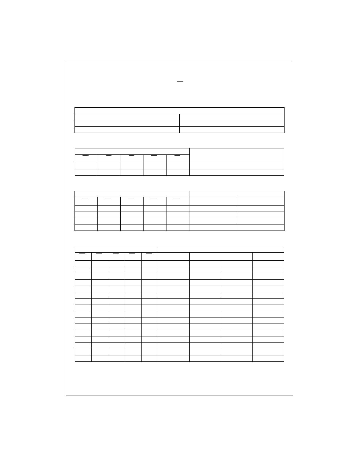
Truth Tables
FSTUD162450
(see Functional Description)
Select Pin
S2 Mode
L Std. NMOS Switch
H Level Shifting Diode Enabled
20-Bit Configuration (S
OE
1
LXXXX 1A
OE
2
= S1 = L)
0
Inputs
OE
3
OE
OE
4
5
Inputs/Outputs
= 1B
1-10
1-10
, 2A
1-10
= 2B
1-10
HXXXX Z
10-Bit Configuration (S
= L, S1 = H)
0
Inputs Inputs/Outputs
OE
LXXLX 1A
LXXHX 1A
HXXLX Z 2A
OE
1
OE
2
OE
3
OE
4
5
1A
1-10
= 1B
= 1B
X
= 1B
X
1-10
X
X
2A
1-10
2AX = 2B
= 2B
= 2B
X
Z
HXXHX Z Z
5-Bit Configuration (S
= H, S1 = L)
0
Inputs Inputs/Outputs
OE2OE3OE4OE51A
OE
1
LLLLX1A
LLLHX1A
LLHLX1A
LLHHX1A
LHLLX1A
LHLHX1A
LHHLX1A
LHHHX1A
HLLLX Z 1A
HLLHX Z 1A
HLHLX Z 1A
HLHHX Z 1A
HHL LX Z Z 2A
HHLHX Z Z 2A
HHHLX Z Z Z 2A
1-5
, 1B
= 1B
x
= 1B
x
= 1B
x
= 1B
x
= 1B
x
= 1B
x
= 1B
x
= 1B
x
1-5
1A
, 1B
6-10
1Ay = 1B
x
1Ay = 1B
x
1Ay = 1B
x
1Ay = 1B
x
x
x
x
x
Z2A
Z2A
ZZ2A
ZZZ
= 1B
y
= 1B
y
= 1B
y
= 1B
y
6-10
y
y
y
y
y
y
y
y
2A
, 2B
1-5
2Ax = 2B
2Ax = 2B
Z2A
1-5
2A
6-10
2Ay = 2B
x
x
= 2B
y
ZZ
= 2B
x
= 2B
x
2Ax = 2B
2Ax = 2B
Z2A
2Ay = 2B
x
x
x
x
= 2B
y
2Ay = 2B
= 2B
y
ZZ
= 2B
x
= 2B
x
2Ay = 2B
x
x
= 2B
y
HHHHX Z Z Z Z
1-10
X
X
, 2B
Z
Z
Z
Z
6-10
y
y
y
y
y
y
y
y
www.fairchildsemi.com 4
 Loading...