

Fairchild Semiconductor FSTUD16211 Datasheet

FSTUD16211
FSTUD16211 24-Bit Bus Switch with
June 2000
Revised August 2001
24-Bit Bus Switch with
−2V Undershoot Protection
and Level Shifting
General Description
The Fairchild Switch FSTUD16211 provides 24-bits of
high-speed CMOS TTL- compatible bu s switching. T he low
on resistance of the switch allows inputs to be connected to
outputs without adding propagation delay or generating
additional ground b ounce noise. A diode to V
integrated into the circuit to allow for leve l shifting b etween
5V inputs and 3.3V outputs.
The device is organ ized as a 12-bit or 24-bit b us switch.
When OE
nected to Port 1B. When OE
to Port 2B. Whe n OE
exists between the A and B Ports. The A and B Ports have
“undershoot hardened” circuit protection to support an
extended range to 2.0V below ground. Fairchild’s integrated Undershoot Hardened Circuit (UHC
undershoot at the I/O’s, and respon ds by preventing voltage differentials from developing and turning on the switch.
is LOW, the switch is ON and Port 1A is con-
1
is LOW, Port 2A is connected
2
is HIGH, a high impedance state
1/2
has been
CC
) senses
Ordering Code:
Order Number Package Number Package Description
FSTUD16211GX
(Note 1)
FSTUD16211MTD MTD56 56-Le ad T hin Shrink Sm all Ou t li n e P ack a ge ( TS S OP ), JEDEC MO-153 , 6. 1mm W id e
Devices also availab l e in Tape and Reel. Specify by appending th e s uffix let t er “X” to the ordering code.
Note 1: BGA package available in Tape and Reel only.
BGA54A
(Preliminary)
54-Ball Fine-Pitch Ball Grid Array (FBGA), JEDEC MO-205, 5.5mm Wide
[TAPE and REEL]
Features
■ Undershoot hardened to −2V (A and B Ports)
■ Voltage level shifting
■ 4
Ω switch connection between two ports
■ Minimal propagation delay through the switch
■ Low l
CC
■ Zero bounce in flow-through mode
■ Control inputs compatible with TTL level
■ See Applications Note AN-5008 for details
■ Also packaged in plastic Fine-Pitch Ball Grid Array
(FBGA) (Preliminary)
−
2V Undershoot Protection and Level Shifting
Logic Diagram
UHC is a trademark of Fairchild Semiconductor Corporation.
© 2001 Fairchild Semiconductor Corporation DS500390 www.fairchildsemi.com
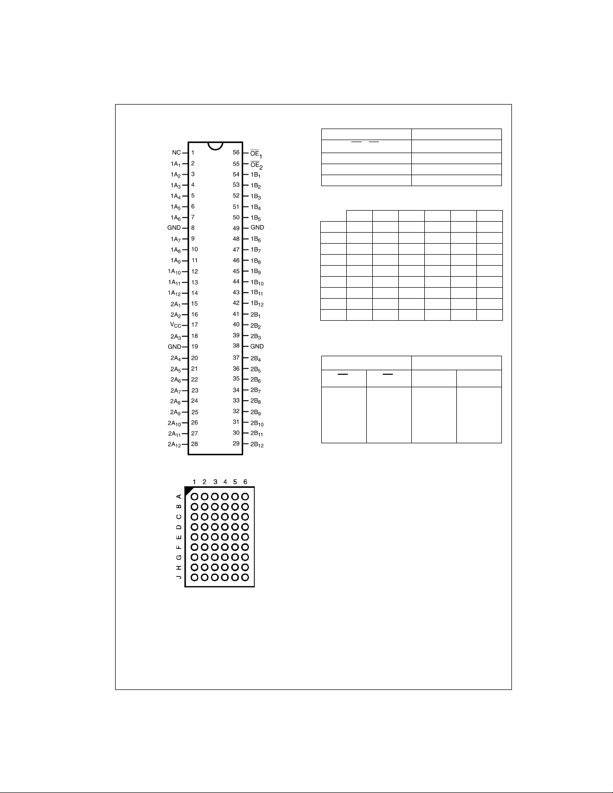
Connection Diagrams
Pin Assignment for TSSOP
FSTUD16211
Pin Descriptions
Pin Name Description
OE
1
, OE
2
Bus Switch Enables
1A, 2A Bus A
1B, 2B Bus B
NC No Connect
Pin Assignment for FBGA
123456
A 1A
1A1NC OE21B11B
2
B 1A41A31A7OE11B31B
C 1A61A5GND 1B71B51B
D 1A101A91A81B81B91B
E 1A121A112A12B11B111B
F 2A42A32A22B22B32B
G 2A62A5VCCGND 2B52B
H 2A82A72A92B92B72B
J 2A122A112A102B102B112B
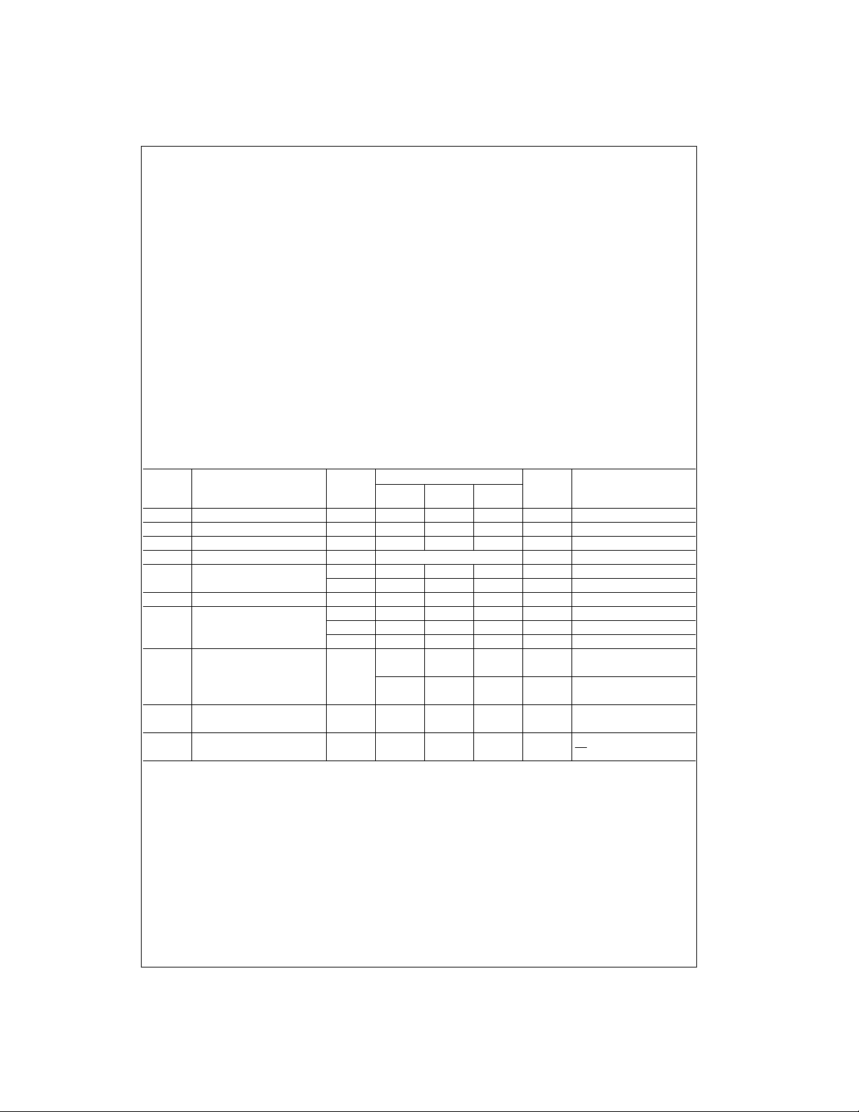
Truth Table
Inputs Inputs/Outputs
OE
1
LL1A = 1B 2A = 2B
LH1A
HLZ2A
HHZZ
OE
2
1A, 1B 2A, 2B
= 1B Z
2
4
6
10
12
4
6
8
12
= 2B
Pin Assignment for FBGA
(Top Thru View)
www.fairchildsemi.com 2
Absolute Maximum Ratings(Note 2) Recommended Operating
Supply Voltage ( VCC) −0.5V to +7.0V
DC Switch Voltage (V
DC Input Control Pin Voltage (V
DC Input Diode Current (l
DC Output (I
DC V
OUT
/GND Current (ICC/I
CC
Storage Temperature Range (T
) (Note 3) −2.0V to +7.0V
S
)(Note 4) −0.5V to +7.0V
IN
) V
< 0V −50 mA
IK
IN
) 128 mA
) +/− 100 mA
GND
) −65°C to +150 °C
STG
Conditions
Power Supply Operating (V
Input Voltage (V
Output Voltage (V
Input Rise and Fall Time (t
Switch Control Input 0 ns/V to 5 ns/V
Switch I/O 0 ns/V to DC
Free Air Operating Temperature (T
Note 2: The “Absolute Maximum Ratings” are those value s beyond which
the safety of the d evice cannot b e guaranteed . The device sh ould not be
operated at these limit s. The parametric values defi ned in the Electrical
Characteristics tables are not guaranteed at the absolute maximum rating.
The “Recomm ended O peratin g Cond itions ” table will defin e the condition s
for actual device operation.
is the voltage observed/applied at either A or B Ports across the
Note 3: V
S
switch.
Note 4: The input and output negative voltage ratings may be exceeded if
the input and ou t put diode current ratings ar e observed.
Note 5: Unused control inputs must be held HIGH or LOW. They may not
float.
(Note 5)
CC)
) 0V to 5.5V
IN
) 0V to 5.5V
OUT
, tf)
r
)-40 °C to +85 °C
A
4.5V to 5.5V
DC Electrical Characteristics
V
Symbol Parameter
V
IK
V
IH
V
IL
V
OH
I
I
I
OZ
R
ON
I
CC
∆ I
V
IKU
Note 6: Typical values are at VCC = 5.0V and TA= +25°C
Note 7: Measured by the voltage drop between A and B pins at the indicated c urrent through the switch. On Resistanc e is determined by the lower of the
voltages on the two (A or B) pins.
Clamp Diode Voltage 4.5 −1.2 V IIN = −18 mA
HIGH Level Input Voltage 4.5–5.5 2.0 V
LOW Level Input Voltage 4.5–5.5 0.8 V
HIGH Level 4.5–5.5 See Figure 4 V
Input Leakage Current 5.5 ±1.0 µA0 ≤ VIN ≤ 5.5V
OFF-STATE Leakage Current 5.5 ±1.0 µA0 ≤ A, B ≤ V
Switch On Resistance 4.5 4 7 Ω VIN = 0V, IIN = 64 mA
(Note 7) 4.5 4 7 Ω V
Quiescent Supply Current
CC
Increase in I
Voltage Undershoot
CC
per Input
CC
(V)
010µAV
4.5 35 50 Ω VIN = 2.4V, IIN = 15 mA
5.5
5.5 2.5 mA
5.5 −2.0 V
TA = −40 °C to +85 °C
Min
Typ
(Note 6)
Max
1.5 mA
10 µA
Units Conditions
= 5.5V
IN
CC
= 0V, IIN = 30 mA
IN
OE1 = OE2 = GND
= VCC or GND, I
V
IN
OE1 = OE2 = V
VIN = VCC or GND, I
One Input at 3.4V
Other Inputs at VCC or GND
0.0 mA ≥ IIN ≥ −50 mA
OE
= 5.5V
1, 2
OUT
CC
OUT
FSTUD16211
= 0
= 0
3 www.fairchildsemi.com
 Loading...