

Fairchild Semiconductor FSTU3125 Datasheet
FSTU3125
FSTU3125 4-Bit Bus Switch with
June 2001
Revised August 2001
4-Bit Bus Switch with
General Description
The Fairchild Switch FST U3125 provides four high-spe ed
CMOS TTL-compatible bus switches. The low On Resistance of the switch allows inputs to be connect ed to outputs without adding propagation delay or generating
additional ground bou nce noise. The A and B Ports are
protected against undershoot to support an extended
range to 2.0V below ground. Fairchild’s integrated Undershoot Hardened Circuit (UHC
I/O and responds by prevent ing voltage differentials from
developing and turning the switch on.
The device is organized as four 1- bit switches with separate OE
inputs. When OE is LOW, the switch is ON and
Port A is connected to Port B. When OE
switch is OPEN and a high-impedance state exists
between the two ports.
) senses undersh oot a t the
−2V Undershoot Protection
Features
■ Undershoot hardened to −2V (A and B Ports)
■ 4
Ω switch connection between two ports
■ Minimal propagation delay through the switch
■ Low l
CC
■ Zero bounce in flow-through mode
■ Control inputs compatible with TTL level
■ See application note s AN-5008 and AN-50 21 for deta ils
on undershoot
is HIGH, the
Ordering Code:
Order Number Package Number Package Description
FSTU3125M M14A 14-Lead Small Outline Integrated Circuit (SOIC), JEDEC MS-012, 0.150" Narrow
FSTU3125QSC MQA16 16-Lead Quarter Size Outline Package (QSOP), JEDEC MO-137, 0.150" Wide
FSTU3125MTC MTC14 14-Lead Thin Shrink Small Outline Package (TSSOP), JEDEC MO-153, 4.4mm Wide
Devices also availab l e in Tape and Reel. Specify by appending th e s uffix let t er “X” to the ordering code.
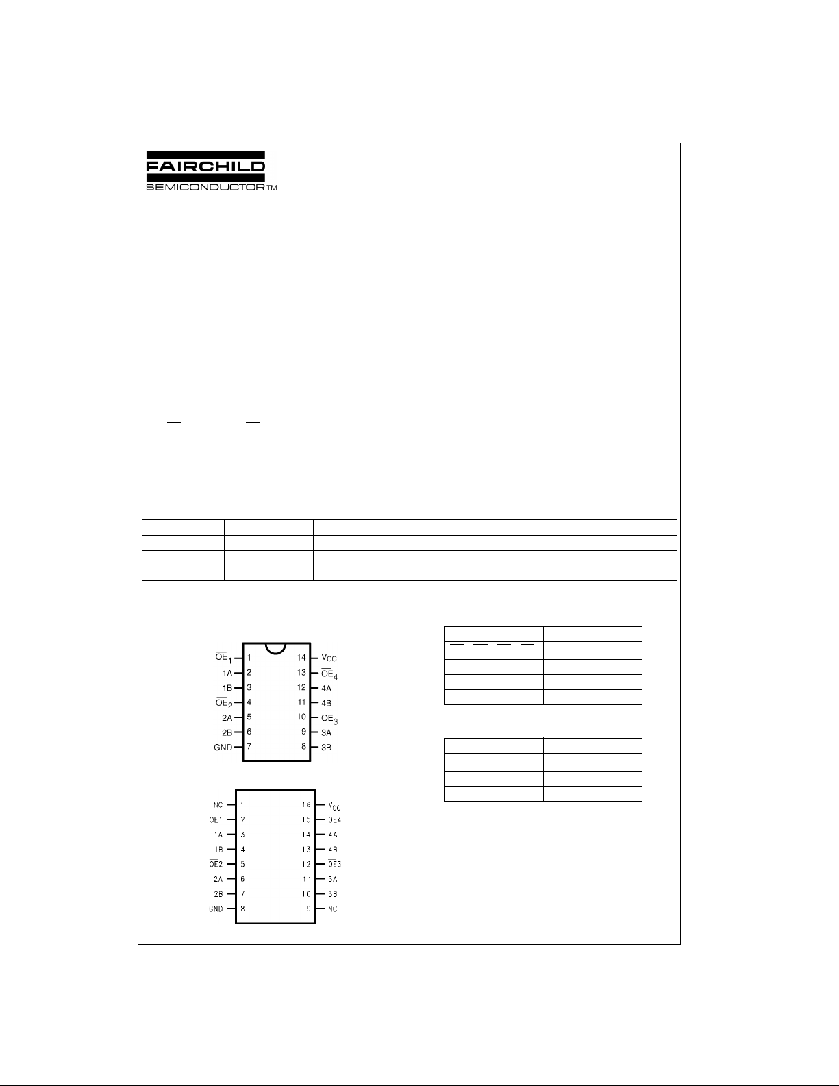
Connection Diagrams
Pin Assignment for SOIC and TSSOP
Pin Descriptions
Pin Name Description
OE
, OE2, OE3, OE4Bus Switch Enables
1
1A, 2A, 3A, 4A Bus A
1B, 2B, 3B, 4B Bus B
NC Not Connected
−
2V Undershoot Protection
Truth T able
Inputs Inputs/Outputs
OE
Pin Assignment for QSOP
© 2001 Fairchild Semiconductor Corporation DS500449 www.fairchildsemi.com
LA
HZ
A,B
= B
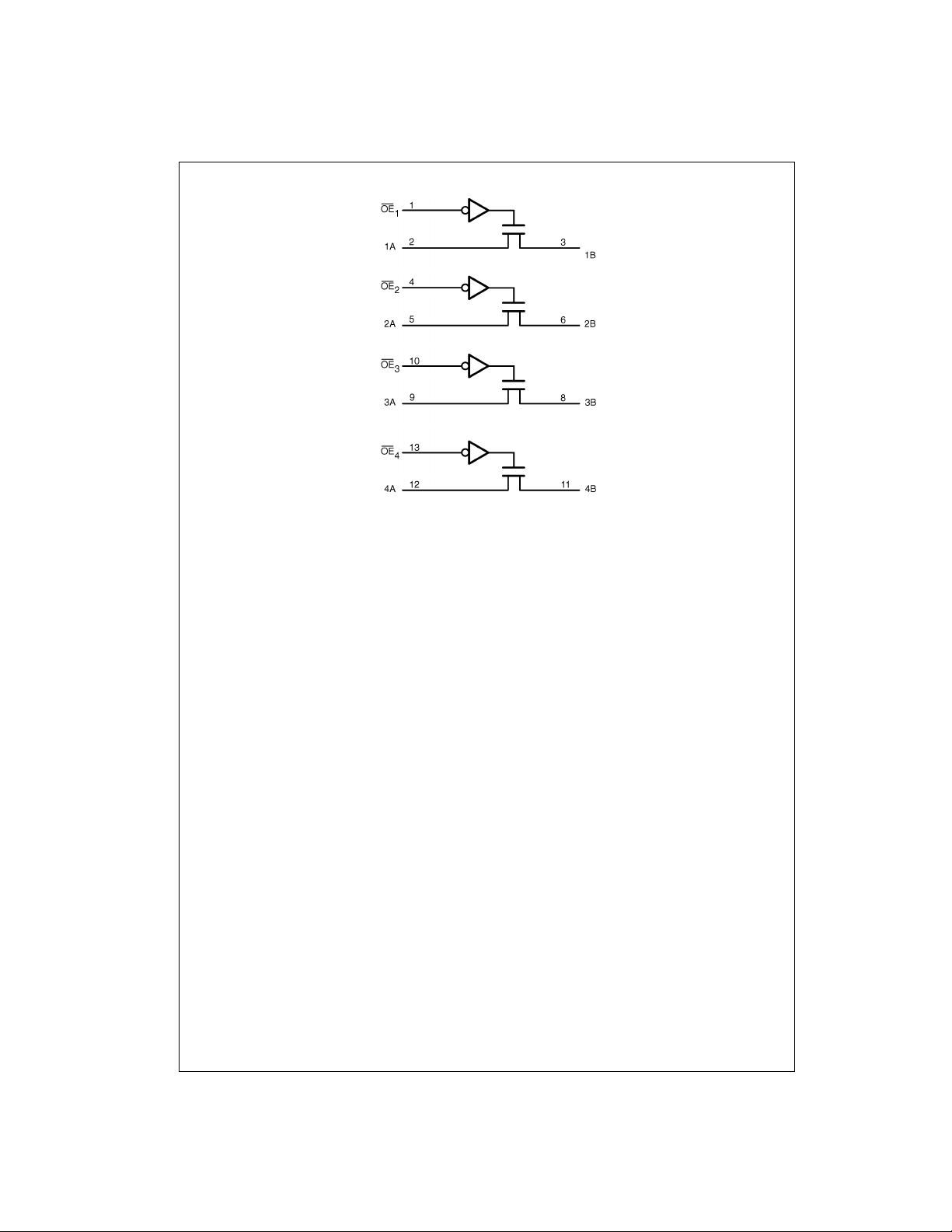
Logic Diagram
FSTU3125
www.fairchildsemi.com 2
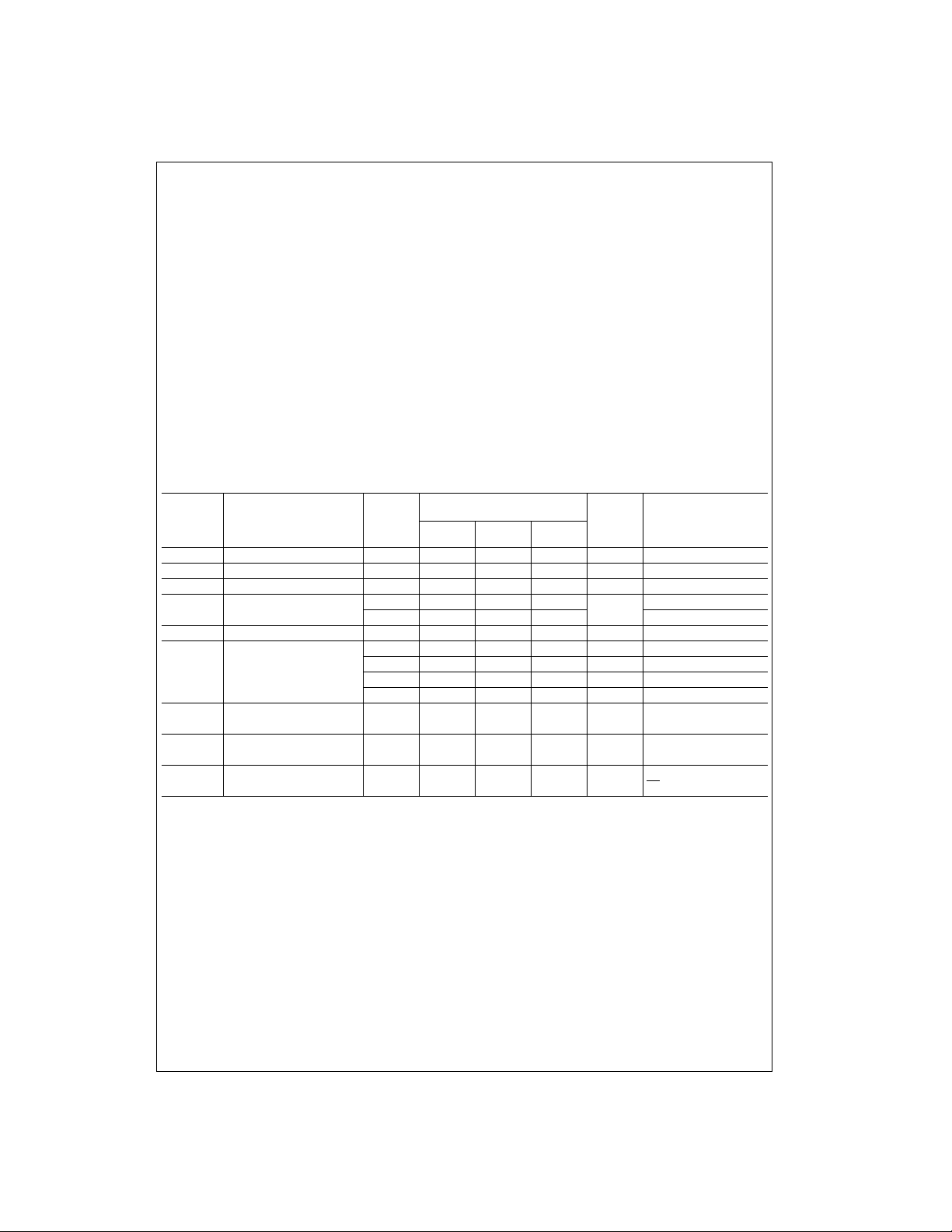
Absolute Maximum Ratings(Note 1) Recommended Operating
Supply Voltage (VCC) −0.5V to +7.0V
DC Switch Voltage (V
DC Input Voltage (V
DC Input Diode Current (l
DC Output (I
DC V
OUT
/GND Current (ICC/I
CC
Storage Temperature Range (T
) −2.0V to +7.0V
S
)(Note 2) −0.5V to +7.0V
IN
) V
< 0V −50 mA
IK
IN
) Sink Current 128 mA
) +/− 100 mA
GND
) −65°C to +150 °C
STG
Conditions
Power Supply Operating (V
Input Voltage (V
Output Voltage (V
Input Rise and Fall Time (t
Switch Control Input 0 ns/V to 5 ns/V
Switch I/O 0 ns/V to DC
Free Air Operating Temperature (T
Note 1: The “Absolute Maximum Ratings” are those value s beyond which
the safety of the d evice cannot b e guaranteed . The device sh ould not be
operated at these limit s. The parametric values defi ned in the Electrical
Characteristics tables are not guaranteed at the absolute maximum rating.
The “Recomm ended O peratin g Cond itions ” table will defin e the condition s
for actual device operation.
Note 2: The input and output negative voltage ratings may be exceeded if
the input and ou t put diode current ratings ar e observed.
Note 3: Unused control inputs must be held HIGH or LOW. They may not
float.
(Note 3)
) 4.0V to 5.5V
CC
) 0V to 5.5V
IN
) 0V to 5.5V
OUT
, tf)
r
) −40 °C to +85 °C
A
DC Electrical Characteristics
FSTU3125
V
Symbol Parameter
V
IK
V
IH
V
IL
I
I
I
OZ
R
ON
I
CC
∆I
CC
V
IKU
Note 4: Typical values are at VCC = 5.0V and TA = +25°C
Note 5: Measured by the voltage drop between A and B pins at the indicated c urrent through the switch. On Resistanc e is determined by the lower of the
voltages on the two (A or B) pins.
Clamp Diode Voltage 4.5 −1.2 V IIN = −18 mA
HIGH Level Input Voltage 4.0–5.5 2.0 V
LOW Level Input Voltage 4.0–5.5 0.8 V
Input Leakage Current 5.5 ±1.0
OFF-STATE Leakage Current 5.5 ±1.0 µA0 ≤ A, B ≤ V
Switch On Resistance 4.5 4 7 Ω VIN = 0V, IIN = 64 mA
(Note 5) 4.5 4 7 Ω VIN = 0V, IIN = 30 mA
Quiescent Supply Current 5.5 3 µAVIN = VCC or GND,
Increase in I
Voltage Undershoot 5.5 −2.0 V 0.0 mA ≥ IIN ≥ −50 mA
per Input 5.5 2.5 mA One input at 3.4V.
CC
CC
(V)
010V
4.5 8 15 Ω V
4.0 11 20 Ω V
TA = −40 °C to +85 °C
Min Typ
(Note 4)
Max
Units Conditions
0 ≤ VIN ≤ 5.5V
µA
= 5.5V
IN
CC
= 2.4V, IIN = 15 mA
IN
= 2.4V, IIN = 15 mA
IN
I
= 0
OUT
Other inputs at VCC or GND
= 5.5V
OE
3 www.fairchildsemi.com
 Loading...