

Fairchild Semiconductor FSTU16861 Datasheet
FSTU16861
FSTU16861 20-Bit Bus Switch with
May 2001
Revised May 2001
20-Bit Bus Switch with
General Description
The Fairchild Switch FS TU16861 provide s 20-Bits of hi ghspeed CMOS TTL-compatible bus switching. The low On
Resistance of the switch allows inputs to be connected to
outputs without adding propagation delay or generating
additional ground bounce noise.
The device is organ ized as a 10-bit or 20-Bit bus switch.
When OE
nected to Port 1B. When OE
to Port 2B. When OE
exists between the A and B Ports . The A an d B Ports a re
protected against undershoot to support an extended
range to 2.0V below ground. Fairchild’s integrated Undershoot Hardened Circuit (UHC
I/O and responds by prevent ing voltage differentials from
developing and turnin g the switch on. When OE
the switch is OPEN and a high-impedance state exists
between the two ports.
is LOW, the switch is ON and Port 1A is con-
1
is LOW, Port 2A is connected
2
is HIGH, a high imped ance state
X
) senses undersh oot a t the
−2V Undershoot Protection
Features
■ Undershoot hardened to −2V (A and B Ports)
Ω switch connection between two ports
■ 4
■ Minimal propagation delay through the switch
■ Low l
CC
■ Zero bounce in flow-through mode
■ Control inputs compatible with TTL level
■ See Application Note AN-5008 for details
is HIGH,
Ordering Code:
Order Number Package Number Package Description
FSTU16861MTD MTD48 48-Lead Thin Shrink Small Outline Package (TSSOP), JEDEC MO-153, 6.1mm Wide
Devices also availab l e in Tape and Reel. Specify by appending th e s uffix let t er “X” to the ordering code.
−
2V Undershoot Protection
UHC is a trademark of Fairchild Semiconductor Corporation.
© 2001 Fairchild Semiconductor Corporation DS500422 www.fairchildsemi.com
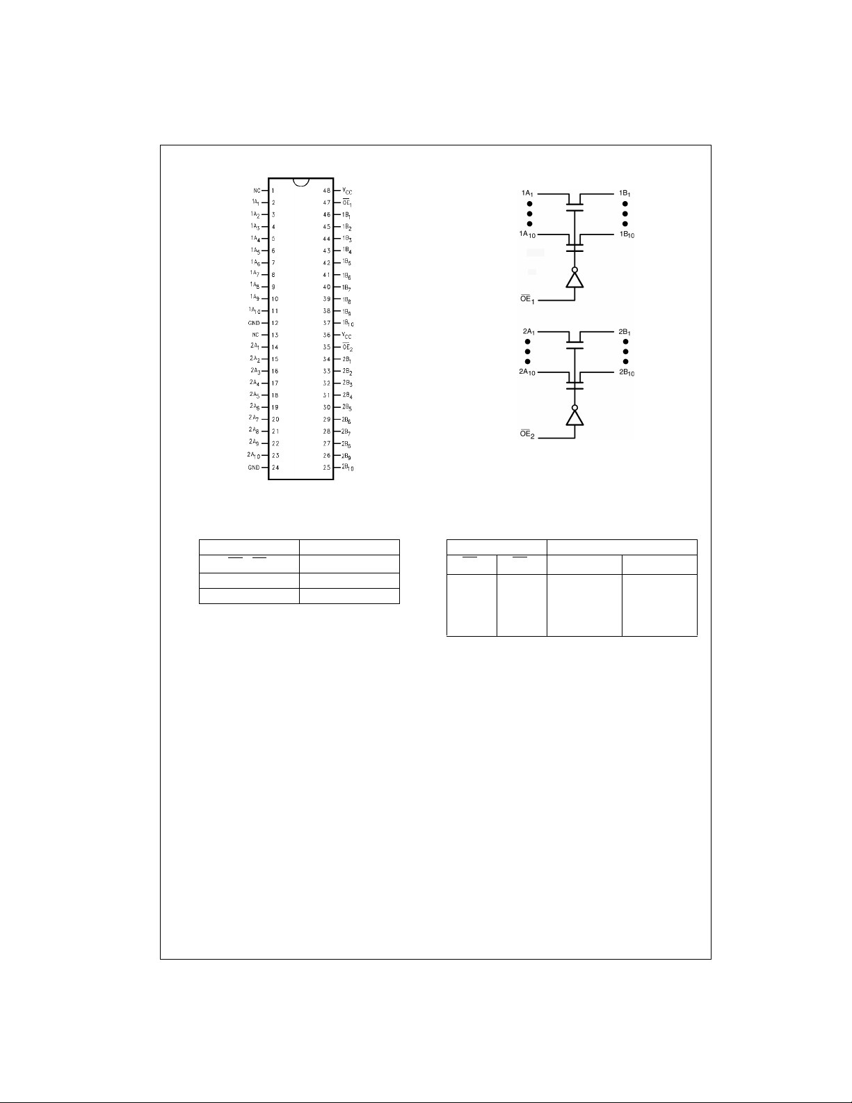
Connection Diagram Logic Diagram
FSTU16861
Pin Descriptions Truth Table
Pin Name Description
OE
1A
1B
1
n
n
, OE
, 2A
, 2B
n
n
2
Bus Switch Enables
Bus A
Bus B
Inputs Inputs/Outputs
OE
1
LL1A
LH1A
HL Z 2A
HH Z Z
H = HIGH Voltage Level
L = LOW Voltage Level
Z = High Impedance
OE
2
1A, 1B 2A, 2B
= 1B 2A = 2B
= 1B Z
= 2B
www.fairchildsemi.com 2
 Loading...