

Fairchild Semiconductor FSTU162211 Datasheet

FSTU162211
Preliminary
June 2001
Revised June 2001
FSTU162211 24-Bit Bus Switch with
(Preliminary)
24-Bit Bus Switch with
and 25
General Description
The Fairchild Switch FSTU162211 provides 24-bits of highspeed CMOS TTL-compatible bus switching. The low On
Resistance of the switch allows inputs to be connected to
outputs without adding propagation delay or generating
additional ground bounce noise.
The device is organ ized as a 12-bit or 24-bit b us switch.
When OE
nected to Port 1B. When OE
to Port 2B. The A and B Ports are protected against under-
shoot to support an extend ed rang e to 2.0V be low gr ound.
Fairchild’s integrated Undershoot Hardened Circuit
(UHC
preventing voltage differentials from developing and turning the switch on.
The FSTU162211 has equivalent 25
reduce signal-reflection noise, eliminating the need for
external terminating resistors.
Ω Series Resistors in Outputs (Preliminary)
is LOW, the switch is ON and Port 1A is con-
1
) senses undershoot at the I/O and responds by
is LOW, Port 2A is connected
2
Ω series resistors to
−2V Undershoot Protection
Features
■ Undershoot hardened to −2V (A and B Ports)
■ Slower output enable times to prevent signal disruption
■ 25
Ω switch connection between two ports
■ Minimal propagation delay through the switch
■ Low l
CC
■ Zero bounce in flow-through mode
■ Control inputs compatible with TTL level
■ See Applications Note AN-5008 for details
Ordering Code:
Order Number Package Num ber Package Description
FSTU162211MTD MTD56 56-Lead Thin Shrink Small Outline Package (TSSOP), JEDEC MO-153, 6.1mm Wide
Devices also availab l e in Tape and Reel. Specify by appending th e s uffix let t er “X” to the ordering code.
−
2V Undershoot Protection and 25
Ω
Series Resistors in Outputs
UHC is a trademark of Fairchild Semiconductor Corporation.
© 2001 Fairchild Semiconductor Corporation DS500064 www.fairchildsemi.com
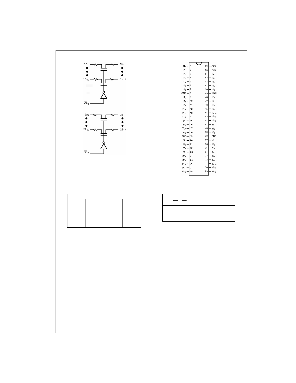
Logic Diagram Connection Diagram
FSTU162211
Preliminary
Truth Table Pin Descriptions
Inputs Inputs/Outputs
OE
LL1A
LH1A
HLZ2A
HHZZ
OE
1
1A, 1B 2A, 2B
2
= 1B 2A = 2B
= 1B Z
= 2B
Pin Name Description
OE
, OE
1
2
1A, 2A Bus A
1B, 2B Bus B
NC No Connect
Bus Switch Enables
www.fairchildsemi.com 2
 Loading...