

Fairchild Semiconductor FQI28N15 Datasheet
FQB28N15 / FQI28N15
150V N-Channel MOSFET
December 2000
QFET
QFET
QFETQFET
FQB28N15 / FQI28N15
TM
General Description
These N-Channel enhancement mode power field effect
transistors are produced using Fairchild’s proprietary,
planar stripe, DMOS technology.
This advanced technology is especially tailored to minimize
on-state resistance, provide superior switching
performance, and withstand high energy pulse in the
avalanche and commutation modes. These devices are
well suited for low voltage applications such as audio
amplifiers, high efficiency switching for DC/DC converters,
DC motor control, and uninterrupted power supplies.
D
G
S
D2-PAK
FQB Series
Absolute Maximum Ratings T
Symbol Parameter FQB28N15 / FQI28N15 Units
V
DSS
I
D
I
DM
V
GSS
E
AS
I
AR
E
AR
dv/dt Peak Diode Recovery dv/dt
P
D
, T
T
J
STG
T
L
Drain-Source Voltage 150 V
Drain Current
Drain Current - Pulsed
Gate-Source Voltage ± 25 V
Single Pulsed Avalanche Energy
Avalanche Current
Repetitive Avalanche Energy
Power Dissipation (TA = 25°C) *
Power Dissipation (T
Operating and Storage Temperature Range -55 to +175 °C
Maximum lead temperature for soldering purposes,
1/8" from case for 5 seconds
G
D
S
= 25°C unless otherwise noted
C
- Continuous (T
- Continuous (T
= 25°C)
C
- Derate above 25°C 1.12 W/°C
= 25°C)
C
= 100°C)
C
Features
• 28A, 150V, R
• Low gate charge ( typical 40 nC)
• Low Crss ( typical 50 pF)
• Fast switching
• 100% avalanche tested
• Improved dv/dt capability
• 175°C maximum junction temperature rating
I2-PAK
FQI Series
(Note 1)
(Note 2)
(Note 1)
(Note 1)
(Note 3)
= 0.09Ω @VGS = 10 V
DS(on)
G
28 A
19.8 A
112 A
300 mJ
28 A
16.8 mJ
5.5 V/ns
3.75 W
168 W
300 °C
D
!
!
"
"
"
"
!
!
"
!
!
"
"
"
!
!
S
Thermal Characteristics
Symbol Parameter Typ Max Units
R
θJC
R
θJA
R
θJA
* When mounted on the minimum pad size recommended (PCB Mount)
©2000 Fairchild Semiconductor International
Thermal Resistance, Junction-to-Case -- 0.89 °C/W
Thermal Resistance, Junction-to-Ambient * -- 40 °C/W
Thermal Resistance, Junction-to-Ambient -- 62.5 °C/W
Rev. A2, December 2000
FQB28N15 / FQI28N15
Electrical Characteristics T
= 25°C unless otherwise noted
C
Symbol Parameter Test Conditions Min Typ Max Units
Off Characteristics
BV
DSS
∆BV
DSS
/ ∆T
I
DSS
I
GSSF
I
GSSR
Drain-Source Breakdown Voltage
Breakdown Voltage Temperature
Coefficient
J
Zero Gate Voltage Drain Current
Gate-Body Leakage Current, Forward
Gate-Body Leakage Current, Reverse
= 0 V, ID = 250 µA
V
GS
I
= 250 µA, Referenced to 25°C
D
V
= 150 V, VGS = 0 V
DS
V
= 120 V, TC = 150°C
DS
V
= 25 V, VDS = 0 V
GS
= -25 V, VDS = 0 V
V
GS
150 -- -- V
-- 0.17 -- V/°C
-- -- 1 µA
-- -- 10 µA
-- -- 100 nA
-- -- -100 nA
On Characteristics
V
R
g
FS
GS(th)
DS(on)
Gate Threshold Voltage
Static Drain-Source On-Resistance
Forward Transconductance
V
= VGS, ID = 250 µA
DS
= 10 V, ID = 14 A
V
GS
= 40 V, ID = 14 A
V
DS
(Note 4)
2.0 -- 4.0 V
-- 0.067 0.09 Ω
-- 18.5 -- S
Dynamic Characteristics
C
iss
C
oss
C
rss
Input Capacitance
Output Capacitance -- 260 340 pF
Reverse Transfer Capacitance -- 50 65 pF
V
= 25 V, VGS = 0 V,
DS
f = 1.0 MHz
-- 1250 1600 pF
Switching Characteristics
t
d(on)
t
r
t
d(off)
t
f
Q
Q
Q
g
gs
gd
Turn-On Delay Time
Turn-On Rise Time -- 180 370 ns
Turn-Off Delay Time -- 100 210 n s
Turn-Off Fall Time -- 115 240 ns
Total Gate Charge
Gate-Source Charge -- 7.9 -- nC
Gate-Drain Charge -- 20 -- nC
V
= 75 V, ID = 28 A,
DD
R
= 25 Ω
G
= 120 V, ID = 28 A,
V
DS
V
GS
= 10 V
(Note 4, 5)
(Note 4, 5)
-- 17 45 ns
-- 40 52 nC
Drain-Source Diode Characteristics and Maximum Ratings
I
S
I
SM
V
SD
t
rr
Q
rr
Notes:
1. Repetitive Rating : Pulse width limited by maximum junction temperature
2. L = 0.64mH, IAS = 28A, VDD = 25V, RG = 25 Ω, Starting TJ = 25°C
3. ISD ≤ 28A, di/dt ≤ 300A/us, VDD ≤ BV
4. Pulse Test : Pulse width ≤ 300µs, Duty cycle ≤ 2%
5. Essentially independent of operating temperature
©2000 Fairchild Semiconductor International
Maximum Continuous Drain-Source Diode Forward Current -- -- 28 A
Maximum Pulsed Drain-Source Diode Forward Current -- -- 112 A
= 0 V, IS = 28 A
Drain-Source Diode Forward Voltage
Reverse Recovery Time
Reverse Recovery Charge -- 0.4 -- µC
Starting TJ = 25°C
DSS,
V
GS
= 0 V, IS = 28 A,
V
GS
dI
/ dt = 100 A/µs
F
-- -- 1.5 V
-- 100 -- ns
(Note 4)
Rev. A2, December 2000
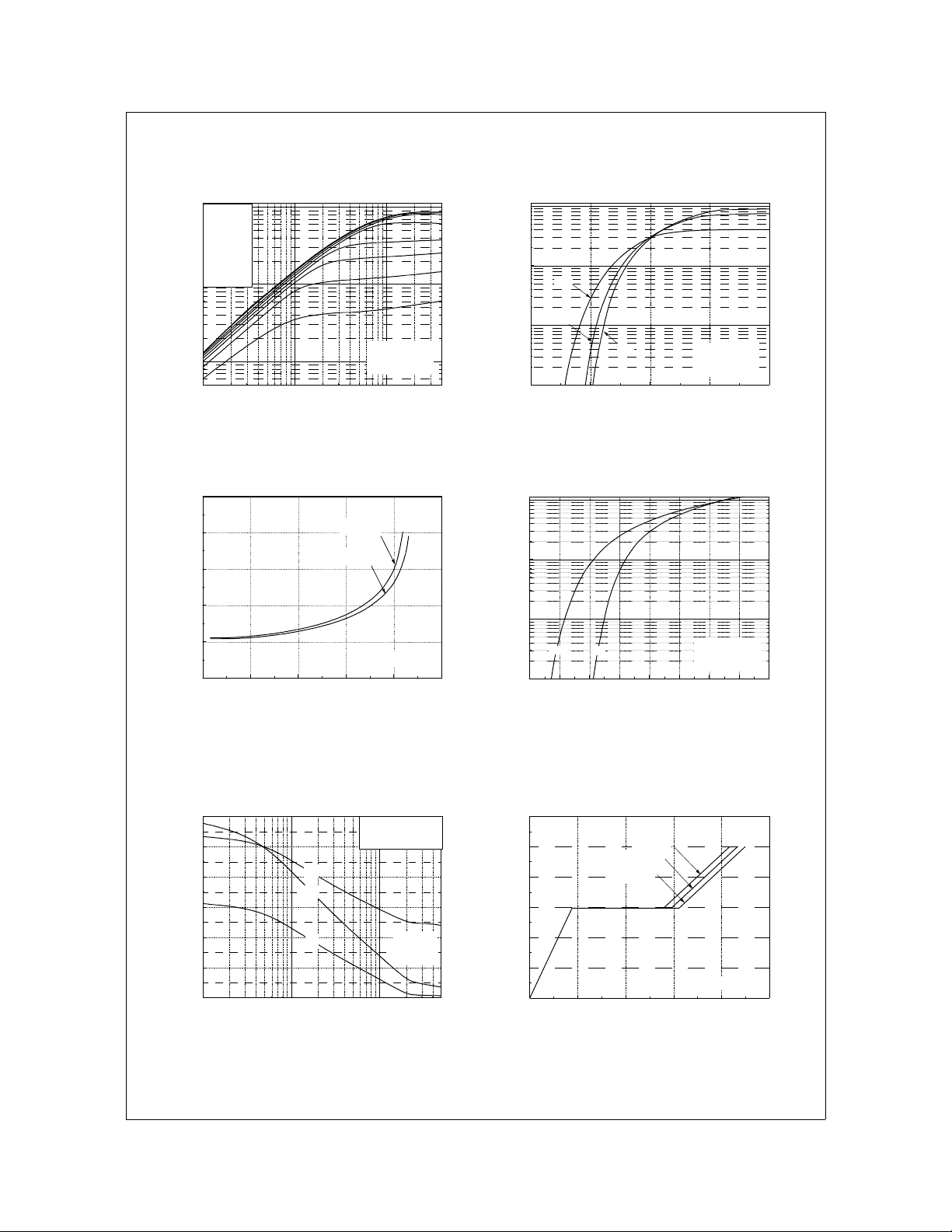
Typical Characteristics
FQB28N15 / FQI28N15
※
Notes :
1. 250μs Pulse Te st
℃
2. T
= 25
C
0
10
1
10
10
10
, Drain Current [A]
D
I
10
2
V
Top : 15.0 V
10.0 V
8.0 V
7.0 V
6.0 V
5.5 V
5.0 V
Bottom : 4.5 V
1
0
-1
10
GS
VDS, Drain - S ou r ce V o lta g e [V ]
300
240
],
Ω
180
[m
DS(ON)
120
R
Drain-Source On-Resistance
60
0
0 20406080100
VGS = 10V
VGS = 20V
※
Note : T
= 25
J
ID , Drain Curren t [A ]
2
10
1
10
℃
175
℃
25
0
10
, Drain Current [A]
D
I
-1
10
246810
℃
-55
※
Notes :
1. V
= 40V
DS
2. 250μs Pulse Test
VGS, Gate-Source V oltage [V]
Figure 2. Transfer CharacteristicsFigure 1. On-Region Char act er i stic s
2
10
1
10
0
10
, Reve rse Drain Cu rren t [A ]
DR
℃
I
℃
175
-1
10
0.2 0.4 0.6 0.8 1.0 1.2 1.4 1.6 1.8
℃
25
VSD, Sou r c e-Drain voltag e [V]
※
Notes :
1. V
= 0V
GS
2. 250μs Pulse Test
Figure 3. On-Resistance Variation vs.
Drain Current and Gate Voltage
3000
2500
2000
1500
1000
Capacitance [pF]
500
0
-1
10
Figure 5. Capacitance Characteristics Figure 6. Gate Charge Ch a ra ct eristics
©2000 Fairchild Semiconductor International
C
C
C
C
iss
C
oss
C
rss
0
10
VDS, Drain-Source Voltage [V]
= Cgs + Cgd (Cds = shorted)
iss
= Cds + C
oss
gd
= C
rss
gd
※
Notes :
1. V
GS
2. f = 1 MHz
1
10
= 0 V
Figure 4. Body Diode Forward Voltage
Variation vs. Source Current
and Temperature
VDS = 30V
VDS = 75V
VDS = 120V
※
Note : I
= 28 A
D
Rev. A2, December 2000
12
10
8
6
4
, Gate-Source Voltage [V]
2
GS
V
0
0 9 18 27 36 45
QG, Tota l Gate Charge [n C]
 Loading...