

Fairchild Semiconductor FQG4902 Datasheet
FQG4902
250V Dual N & P-Channel MOSFET
FQG4902
TM
QFET
General Description
These dual N and P-channel enhancement mode power
field effect transistors are produced using Fairchild’s
proprietary, planar stripe, DMOS technology.
This advanced technology has been especially tailored to
minimize on-state resistance, provide superior switching
performance, and withstand high energy pulse in the
avalanche and commutation mode. These devices are well
suited for electronic lamp ballast based on half bridge.
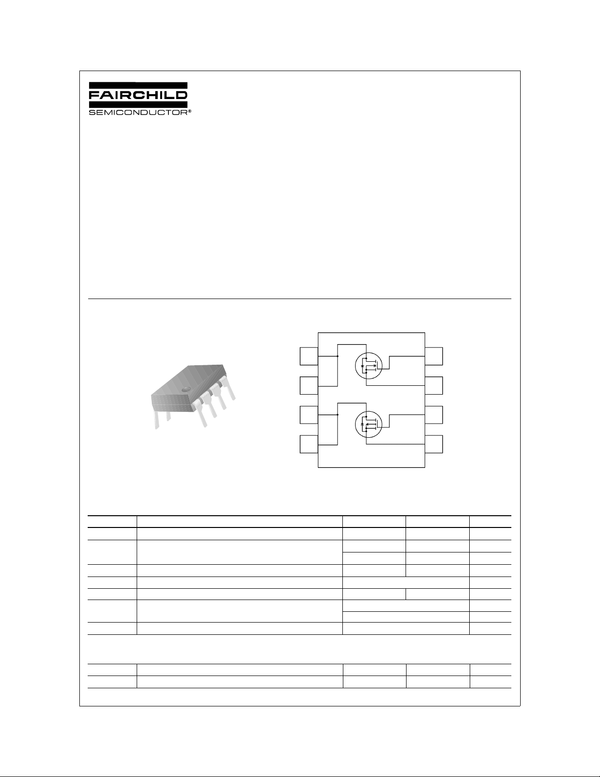
D2
D2
D1
D1
G2
S2
G1
S1
8-DIP
Pin #1
Features
• N-Channel 0.54A, 250V, R
P-Channel -0.54A, -250V, R
• Low gate charge ( typical N-Channel 6.0 nC)
( typical P-Channel 12.0 nC)
• Fast switching
• Improved dv/dt capability
5
6
7
8
= 2.0 Ω @ VGS = 10 V
DS(on)
= 2.0 Ω @ VGS = -10 V
DS(on)
4
3
2
1
Absolute Maximum Ratings T
Symbol Parameter N-Channel P-Channel Units
V
DSS
I
D
I
DM
V
GSS
dv/dt Peak Diode Recovery dv/dt
P
D
T
, T
J
STG
Drain-Source Voltage 250 -250 V
Drain Current
Drain Curent - Pulsed
Gate-Source Voltage ± 30 V
Power Dissipation (TA = 25°C)
- Derate above 25°C 0.011 W/°C
Operating and Storage Temperature Range -55 to +150 °C
- Continuous (T
- Continuous (T
= 25°C unless otherwise noted
A
= 25°C)
A
= 100°C)
A
(Note 1)
(Note 2)
0.54 -0.54 A
0.34 -0.34 A
4.32 -4.32 A
5.5 -5.5 V/ns
1.4 W
Thermal Characteristics
Symbol Parameter Typ Max Units
R
θJA
©2002 Fairchild Semiconductor Corporation Rev. A1, April 2002
Thermal Resistance, Junction-to-Ambient
(Note 5a)
-- 90 °C/W
FQG4902
Electrical Characteristics T
= 25°C unless otherwise noted
A
Symbol Parameter Test Conditions Type Min Typ Max Units
Off Characteristics
BV
∆BV
/ ∆T
I
DSS
I
GSSF
I
GSSR
Drain-Source Breakdown Voltage VGS = 0 V, ID = 250 µA
DSS
V
= 0 V, ID = -250 µA
GS
Breakdown Voltage Temperature
DSS
Coefficient
J
ID = 250 µA,
Referenced to 25°C
I
= -250 µA,
D
Referenced to 25°C
Zero Gate Voltage Drain Current VDS = 250 V, VGS = 0 V
V
= 200 V, TA = 125°C
DS
V
= -250 V, VGS = 0 V
DS
= -200 V, TA = 125°C
V
DS
= 30 V, VDS = 0 V
Gate-Body Leakage Current, Forward
Gate-Body Leakage Current, Reverse
V
GS
= -30 V, VDS = 0 V
V
GS
N-Ch 250 -- -- V
P-Ch -250 -- -- V
N-Ch -- 0.24 -- V/°C
P-Ch -- -0.2 -- V/°C
N-Ch
P-Ch
-- -- 10 µA
-- -- 100 µA
-- -- -10 µA
-- -- -100 µA
All -- -- 100 nA
All -- -- -100 nA
On Characteristics
V
R
g
FS
GS(th)
DS(on)
Gate Threshold Voltage VDS = VGS, ID = 250 µA
V
= VGS, ID = -250 µA
DS
Static Drain-Source On-Resistance VGS = 10 V, ID = 0.27 A
V
= -10 V, ID = -0.27 A
GS
Forward Transconductance VDS = 40 V, ID = 0.27 A
= -40 V, ID = -0.27 A
V
DS
N-Ch 2.0 -- 4.0 V
P-Ch -2.0 -- -4.0 V
N-Ch -- 1.1 2.0 Ω
P-Ch -- 1.5 2.0 Ω
N-Ch -- 1.3 -- S
P-Ch -- 1.1 -- S
Dynamic Characteristics
C
iss
C
oss
C
rss
Input Capacitance
Output Capacitance N-Ch -- 40 55 pF
Reverse Transfer Capacitance N-Ch -- 7 9. 5 pF
Switching Characteristics
t
d(on)
t
r
t
d(off)
t
f
Q
Q
Q
g
gs
gd
Turn-On Delay Time
Turn-On Rise Time N-Ch -- 17 45 ns
Turn-Off Delay Time N-Ch -- 29 70 ns
Turn-Off Fall Time N-Ch -- 23 55 ns
Total Gate Charge N-Channel
Gate-Source Charge N-Ch -- 1.1 -- nC
Gate-Drain Charge N-Ch -- 2.7 -- nC
N-Channel
V
= 25 V, VGS = 0 V,
DS
f = 1.0 MHz
P-Channel
= -25 V, VGS = 0 V,
V
DS
f = 1.0 MHz
N-Channel
= 125 V, ID = 0.54 A,
V
DD
= 25 Ω
R
G
P-Channel
V
= -125 V, ID = -0.54 A,
DD
= 25 Ω
R
G
(Note 3,4)
= 200 V, ID = 0.54 A,
V
DS
V
= 10 V
GS
P-Channel
V
= -200 V, ID = -0.54 A,
DS
V
GS
= -10 V
(Note 3,4)
N-Ch -- 195 250 pF
P-Ch -- 345 445 pF
P-Ch -- 65 85 pF
P-Ch -- 11 14.5 pF
N-Ch -- 5.5 20 ns
P-Ch -- 8.0 25 ns
P-Ch -- 19 50 ns
P-Ch -- 44 100 ns
P-Ch -- 33 75 ns
N-Ch -- 6.0 7.8 nC
P-Ch -- 12.0 15.6 nC
P-Ch -- 2.2 -- nC
P-Ch -- 5.3 -- nC
©2002 Fairchild Semiconductor Corporation
Rev. A1, April 2002
FQG4902
Electrical Characteristics
(Continued)
Symbol Parameter Test Conditions Type Min Typ Max Units
Drain-Source Diode Characteristics and Maximum Ratings
I
S
I
SM
V
SD
t
rr
Q
rr
t
rr
Q
rr
Notes:
1. Repetitive Rating : Pulse width limited by maximum junction temperature
2. ISD ≤ 0.54A, di/dt ≤ 200A/µs, VDD ≤ BV
3. Pulse Test : Pulse width ≤ 300µs, Duty cycle ≤ 2%
4. Essentially independent of operating temperature
5. R
Maximum R
a. 90°C/W when mounted without any pad copper
b. 62.5°C/W when mounted on a 4.5 in2 pad of 2oz copper. In such an environment, the power dissipation can be enhanced up to 2W
Maximum Continuous Drain-Source Diode Forward Current N-Ch -- -- 0.54 A
P-Ch -- -- -0.54 A
Maximum Pulsed Drain-Source Diode Forward Current N-Ch -- -- 4.32 A
P-Ch -- -- -4.32 A
Drain-Source Diode Forward Voltage VGS = 0 V , IS = 0.54 A
V
= 0 V , IS = -0.54 A
GS
= 0 V , IS = 0.54 A,
Reverse Recovery Time
Reverse Recovery Charge -- 189 -- nC
Reverse Recovery Time
Reverse Recovery Charge -- 210 -- nC
Starting TJ = 25°C
DSS,
is the sum of the junction-to-case and case-to-ambient thermal resistance. R
JA
θ
using the different board layouts on 3”x4.5” FR-4 PCB in a still air environment :
JA
θ
V
GS
dI
/ dt = 100 A/µs
F
= 0 V , IS = -0.54 A,
V
GS
/ dt = 100 A/µs
dI
F
θ
(Note 3)
(Note 3)
is determined by the user’s board design
CA
N-Ch -- -- 1.5 V
P-Ch -- -- -5.0 V
N-Ch
P-Ch
-- 90 -- ns
-- 77 -- ns
©2002 Fairchild Semiconductor Corporation
Rev. A1, April 2002
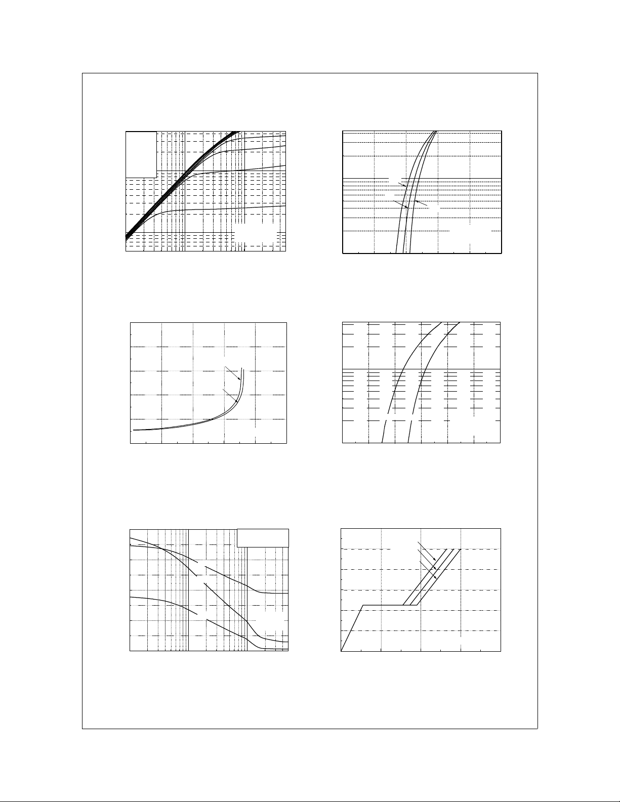
Typical Characteristics : N-Channel
FQG4902
V
GS
Top : 15 .0 V
10.0 V
8.0 V
6.0 V
5.5 V
5.0 V
0
4.5 V
10
Bottom : 4.0 V
, Drain Current [A]
D
I
-1
10
-1
10
0
10
!
Notes :
1. 250#s Pulse Test
"
2. TA = 25
1
10
VDS, Drain-Source Voltage [V]
Figure 1. On-Region Char act er i stic s
10
8
6
],
$
[
4
DS(ON)
R
2
Drain-Source On-Resistance
0
0246810
VGS = 10V
VGS = 20V
ID, Drain Current [A]
!
Note : T
"
= 25
J
0
10
, Drain Current [A]
D
I
-1
10
0246810
"
150
"
25
"
-55
!
Note s :
= 40V
1. V
DS
2. 250#s Pulse Test
VGS , Gate-Source Voltage [V]
Figure 2. Transfer Characteristics
0
10
"
, Reverse Drain Current [A]
DR
I
-1
10
0.2 0.4 0.6 0.8 1.0 1.2 1.4
150
"
25
!
Note s :
1. V
= 0V
GS
2. 250#s Pulse Test
VSD, Sou rce -Drain vo lta ge [V ]
Figure 3. On-Resistance Variati on vs.
Drain Current and Gate Voltage
Figure 4. Body Diode Forward Voltage
Variation vs. Source Current
and Temperature
VDS = 50V
VDS = 125V
VDS = 200V
!
Note : I
= 0.54 A
D
400
300
200
Capacitance [pF]
100
0
-1
10
C
= Cgs + Cgd (Cds = shorted)
iss
= Cds + C
C
oss
gd
C
= C
rss
gd
C
iss
C
oss
C
rss
0
10
!
Note s :
= 0 V
1. V
GS
2. f = 1 MHz
1
10
VDS, Drain-Source Voltage [V]
12
10
8
6
4
, Gate-Source Voltage [V]
GS
2
V
0
02468
QG, Tota l G ate C h arg e [nC]
Figure 5. Capacitance C haracteristics Figure 6. Ga te Ch arge Characteristics
©2002 Fairchild Semiconductor Corporation Rev. A1, April 2002
 Loading...