

Fairchild Semiconductor FPN630A, FPN630 Datasheet
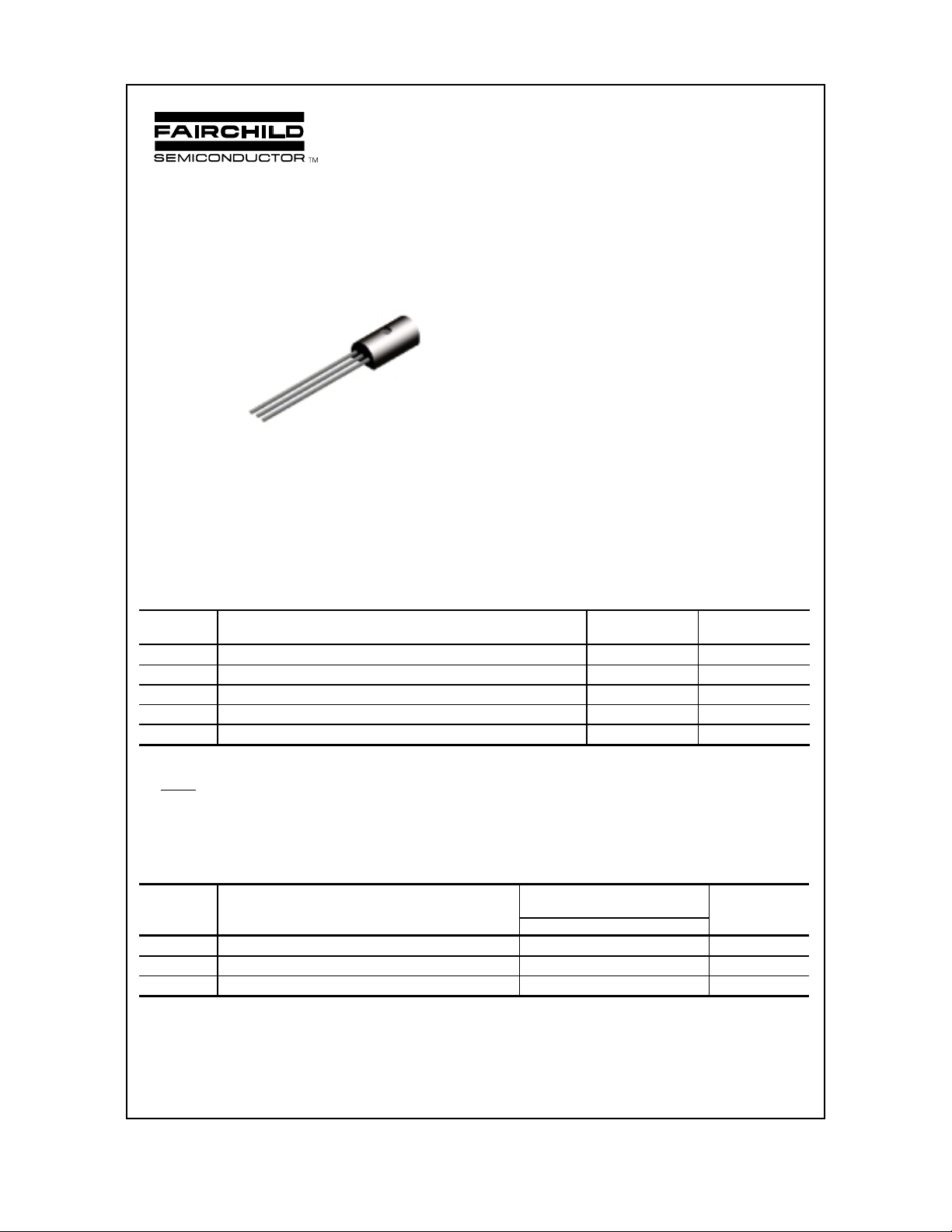
FPN630
FPN630A
FPN630 / FPN630A
C
B
E
TO-226
PNP Low Saturation Transistor
These devices are designed for high current gain and low
saturation voltage with collector currents up to 3.0 A continuous.
Sourced from Process PC.
Absolute Maximum Ratings* TA = 25°C unless otherwise noted
Symbol Parameter Value Units
V
CEO
V
CBO
V
EBO
I
C
TJ, T
stg
*These ratings are limiting values above which the serviceability of any semiconductor device may be impaired.
NOTES:
1) These ratings are based on a maximum junction temperature of 150 degrees C.
2) These are steady state limits. The factory should be consulted on applications involving pulsed or low duty cycle operations.
3) All voltages (V) and currents (A) are negative polarity for PNP transistors.
Collector-Emitter V ol tage 30 V
Collector-Base Voltage 35 V
Emitter-Base Volt age 5.0 V
Collector Current - Continuous 3.0 A
Operating and Storage Junction Temperature Range -55 to +150
C
°
Thermal Characteristics TA = 25°C unless otherwise noted
Symbol Characteristic Max Units
FPN630 / FPN630A
P
D
R
θ
JC
R
θ
JA
1999 Fairchild Semiconductor Corporation
Total Device Dissipation 1.0 W
Thermal Resistance, Junction to Case 50
Thermal Resistance, Junction to Ambient 125
°C/W
°
C/W
PNP Low Saturation Transistor
(continued)
Electrical Characteristics TA = 25°C unless otherwise noted
Symbol Parameter Test Conditions Min Max Units
OFF CHARACTERISTICS
BV
CEO
BV
CBO
BV
EBO
I
CBO
I
EBO
ON CHARACTERISTICS*
h
FE
V
sat
CE(
V
sat
BE(
V
BE(on)
Collector-Emitter Breakdown
IC = 10 mA, IB = 0 30 V
Voltage
Collector-Base Breakdown Voltage
Emitter-Base Breakdown Voltage
Collector Cutoff Current VCB = 30 V, I
Emitter Cutoff Current VEB = 4.0 V, I
DC Current Gain
Collector-Emitter S aturation Voltage
)
I
= 100 µA, IE = 0
C
I
= 100 µA, IC = 0
E
= 0
E
= 30 V, I
V
CB
= 100 mA, VCE = 2.0 V
I
C
I
= 1.0 A, VCE = 2.0 V
C
= 2.0 A, VCE = 2.0 V
I
C
= 1.0 A, IB = 100 mA
I
C
= 0, TA = 100°C
E
= 0 100 nA
C
630
630A
630
35 V
5.0 V
100
250
60
40
630A
I
= 2.0 A, IB = 200 mA
Base-Emitter Saturation Voltage IC = 1.0 A, IB = 100 mA 1.25 V
)
C
Base-Emitter Saturation Voltage IC = 1.0 A, VCE = 2.0 V 1.0 V
100
10
300
250
500
nA
µ
mV
mV
mV
A
FPN630 / FPN630A
SMALL SIGNAL CHARACTERISTICS
C
obo
F
T
Output Capacitance VCB = 10 V, IE = 0, f = 1.0 MHz 100 pF
Transition Frequency IC = 100 mA, VCE = 5.0 V,
f = 100 MHz
*Pulse T est: Pulse Width ≤ 300 µs, Duty Cycle ≤ 2.0%
NOTE: All voltages (V) and currents (A) are negative polarity for PNP transistors.
100 MHz
 Loading...