

Fairchild Semiconductor FPN560A, FPN560 Datasheet
FPN560
FPN560A
FPN560 / FPN560A
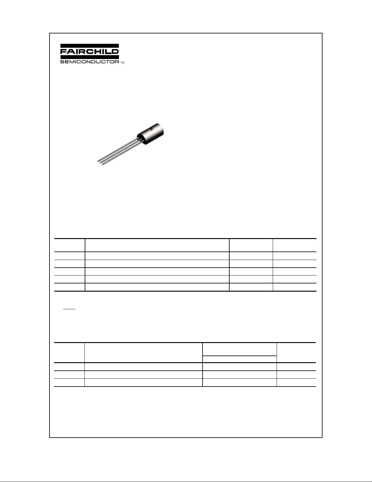
C
B
E
TO-226
NPN Low Saturation Transistor
These devices are designed for high current gain and low
saturation voltage with collector currents up to 3.0 A continuous.
Sourced from Process NA.
Absolute Maximum Ratings* TA = 25°C unless otherwise noted
Symbol Parameter Value Units
V
CEO
V
CBO
V
EBO
I
C
TJ, T
stg
*These ratings are limiting values above which the serviceability of any semiconductor device may be impaired.
NOTES:
1) These ratings are based on a maximum junction temperature of 150 degrees C.
2) These are steady state limits. The factory should be consulted on applications involving pulsed or low duty cycle operations.
Thermal Characteristics TA = 25°C unless otherwise noted
Collector-Emitter V ol tage 60 V
Collector-Base Voltage 80 V
Emitter-Base Volt age 5.0 V
Collector Current - Continuous 3.0 A
Operating and Storage Junction Temperature Range -55 to +150
C
°
Symbol Characteristic Max Units
FPN560 / FPN560A
P
D
R
θ
JC
R
θ
JA
1999 Fairchild Semiconductor Corporation
Total Device Dissipation 1.0 W
Thermal Resistance, Junction to Case 50
Thermal Resistance, Junction to Ambient 125
°C/W
°C/W

NPN Low Saturation Transistor
(continued)
Electrical Characteristics TA = 25°C unless otherwise noted
Symbol Parameter Test Conditions Min Max Units
OFF CHARACTERISTICS
BV
CEO
BV
CBO
BV
EBO
I
CBO
I
EBO
ON CHARACTERISTICS*
h
FE
V
sat
CE(
V
sat
BE(
V
BE(on)
Collector-Emitter Breakdown
IC = 10 mA, IB = 0 60 V
Voltage
Collector-Base Breakdown Voltage
Emitter-Base Breakdown Voltage
I
= 100 µA, IE = 0
C
I
= 100 µA, IC = 0
E
Collector Cutoff Current VCB = 30 V, I
= 30 V, I
V
CB
Emitter Cutoff Current VEB = 4.0 V, I
DC Current Gain IC = 100 mA, VCE = 2.0 V
I
= 500 mA, VCE = 2.0 V
C
I
= 1.0 A, VCE = 2.0 V
C
= 2.0 A, VCE = 2.0 V
I
Collector-Emitter Saturation Voltage IC = 1.0 A, IB = 100 mA
)
C
= 2.0 A, IB = 200 mA
I
C
= 0
E
= 0, TA = 100°C
E
= 0 100 nA
C
560
560A
560
80 V
5.0 V
70
100
250
80
40
560A
Base-Emitter Saturation Voltage IC = 1.0 A, IB = 100 mA 1.25 V
)
Base-Emitter Saturation Voltage IC = 1.0 A, VCE = 2.0 V 1.0 V
100
10
300
550
300
350
300
nA
µ
mV
mV
mV
A
FPN560 / FPN560A
SMALL SIGNAL CHARACTERISTICS
C
obo
F
T
Output Capacitance VCB = 10 V, IE = 0, f = 1.0 MHz 30 pF
Transition Frequency IC = 100 mA, VCE = 5.0 V,
*Pulse T est: Pulse Width ≤ 300 µs, Duty Cycle ≤ 2.0%
f = 100 MHz
75 MHz
 Loading...