

Fairchild Semiconductor FPF1006, FPF1005 Datasheet
tm
FPF1005-FPF1006
TM
IntelliMAX
Advanced Load Management Products
FPF1005-FPF1006 IntelliMAX
April 2007
Features
1.2 to 5.5V Input Voltage Range
Typical R
Typical R
ESD Protected, above 2000V HBM
= 50mΩ @ VIN = 5.5V
DS(ON)
= 55mΩ @ VIN = 3.3V
DS(ON)
Applications
PDAs
Cell Phones
GPS Devices
MP3 Players
Digital Cameras
Peripheral Ports
Hot Swap Supplies
RoHS Compliant
PIN 1
General Description
The FPF1005 & FPF1006 are low RDS P-Channel MOSFET
load switches with CMOS controlled turn-on targeting small
package load switch applications. The input voltage range
operates from 1.2V to 5.5V. Switch control is by a logic
input (ON) capable of interfacing directly with low voltage
control signals. In FPF1006, 120Ω on-chip load resistor is
added for output quick discharge when switch is turned off.
Both FPF1005 & FPF1006 are available in a small 2X2
MicroFET-6 pin plastic package.
TM
Advanced Load Management Products
BOTTOM
TOP
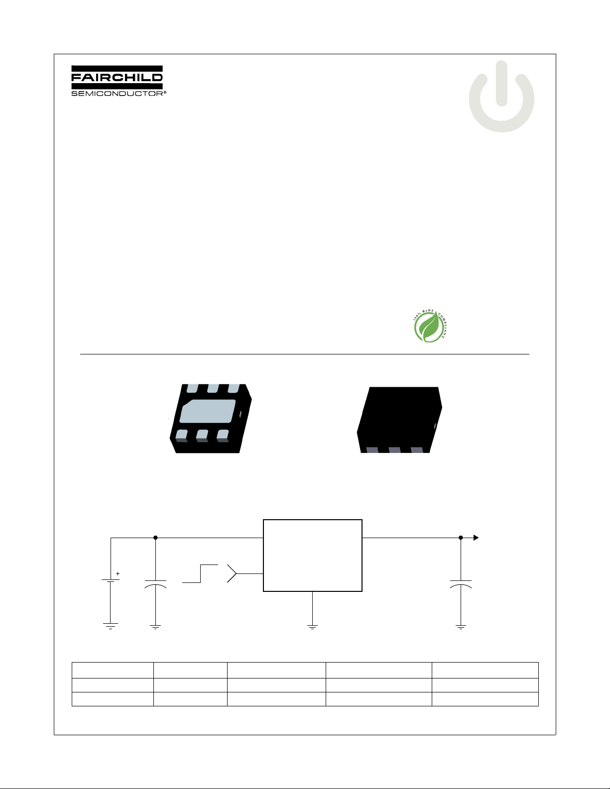
Typical Application Circuit
TO LOAD
V
IN
V
OUT
FPF1005/6
-
OFF ON ON
C
IN
GND
C
OUT
Ordering Information
Part Switch Input Buffer Output Discharge ON Pin Activity
FPF1005 55mΩ, PMOS Schmitt NA Active HI
FPF1006 55mΩ, PMOS Schmitt 120Ω Active HI
©2006 Fairchild Semiconductor Corporation 1 www.fairchildsemi.com
FPF1005-FPF1006 Rev. F
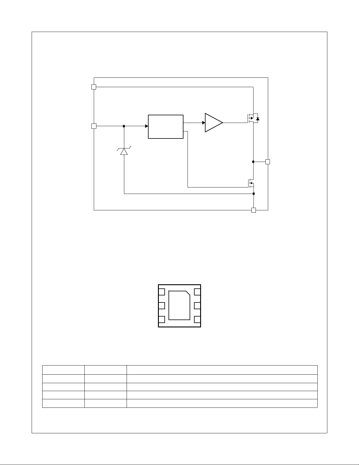
Functional Block Diagram
V
IN
FPF1005-FPF1006 IntelliMAX
Turn-On Slew Rate
Controlled Driver
ON
Pin Configuration
CONTROL
ESD protection
FPF1005/6
GND
LOGIC
6
Output Discharge
(Optional)
ON
1
GND
V
TM
Advanced Load Management Products
OUT
Pin Description
Pin Name Function
4, 5 V
2, 3 V
6 GND Ground
1 ON ON/OFF Control Input
FPF1005-FPF1006 Rev. F
OUT
IN
5
V
OUT
V
4
OUT
MicroFET 2x2 6L BOTTOM
Switch Output: Output of the power switch
Supply Input: Input to the power switch and the supply voltage for the IC
2 www.fairchildsemi.com
V
2
IN
V
3
IN
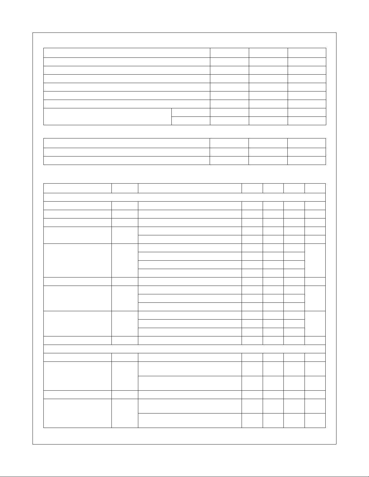
Absolute Maximum Ratings
Parameter Min Max Unit
VIN, V
Maximum Continuous Switch Current 1.5 A
Power Dissipation @ T
Operating Temperature Range -40 85 °C
Storage Temperature -65 150 °C
Thermal Resistance, Junction to Ambient 86 °C/W
Electrostatic Discharge Protection
, ON to GND -0.3 6 V
OUT
= 25°C (Note 1) 1.2 W
A
HBM 2000 V
MM 200 V
Recommended Operating Range
Parameter Min Max Unit
V
IN
Ambient Operating Temperature, T
A
1.2 5.5 V
-40 85 °C
Electrical Characteristics
VIN = 1.2 to 5.5V, TA = -40 to +85°C unless otherwise noted. Typical values are at VIN = 3.3V and TA = 25°C.
Parameter Symbol Conditions Min Typ Max Unit
Basic Operation
Operating Voltage V
Quiescent Current I
Off Supply Current I
Off Switch Current I
On-Resistance R
Output Pull Down Resistance R
ON Input Logic Low Voltage V
ON Input Logic High Voltage V
IN
Q
Q(off)
SD(off)
ON
PD
IL
IH
ON Input Leakage V
Dynamic
Turn on delay t
Turn off delay t
Rise Time t
V
OUT
V
Fall Time t
OUT
ON
OFF
R
F
I
= 0mA, VIN = V
OUT
ON
VON = GND, OUT = open 1 µA
VON = GND, V
= GND, V
V
ON
= 0 @ VIN = 5.5V, TA = 85°C 1 µA
OUT
= 0 @ VIN = 3.3V, TA = 25°C 10 100 nA
OUT
VIN = 5.5V, TA = 25°C 50 70
= 3.3V, TA = 25°C 55 80
V
IN
= 1.5V, TA = 25°C 95 135
V
IN
= 1.2V, TA = 25°C 165 250
V
IN
VIN = 3.3V, VON = 0V, TA = 25°C, FPF1006 75 120 Ω
VIN = 5.5V 1.25
= 4.5V 1.10
IN
= 1.5V 0.50
V
IN
VIN = 5.5V 2.00
= 4.5V 1.75
IN
= 1.5V 0.75
V
IN
= VIN or GND -1 1 µA
ON
VIN = 3.3V, RL = 500Ω, CL = 0.1µF, TA = 25°C 10 µs
VIN = 3.3V, RL = 500Ω, CL = 0.1µF,
T
= 25°C, FPF1005
A
= 3.3V, RL = 500Ω, CL = 0.1µF,
V
IN
R
= 120Ω, TA = 25°C, FPF1006
L_CHIP
VIN = 3.3V, RL = 500Ω, CL = 0.1µF, TA = 25°C 10 µs
VIN = 3.3V, RL = 500Ω, CL = 0.1µF,
T
= 25°C, FPF1005
A
V
= 3.3V, RL = 500Ω, CL = 0.1µF,
IN
R
= 120Ω, TA = 25°C, FPF1006
L_CHIP
1.2 5.5 V
1µA
mΩ
50 µs
10 µs
100 µs
10 µs
FPF1005-FPF1006 IntelliMAX
TM
Advanced Load Management Products
VV
VV
FPF1005-FPF1006 Rev. F
3 www.fairchildsemi.com
 Loading...