

Fairchild Semiconductor FPBL10SH60 Datasheet
©2002 Fairchild Semiconductor Corporation
FPBL10SH60
Rev. B1, February 2002
FPBL10SH60
Smart Power Module (SPM)
General Description
FPBL10SH60 is an advanced smart power module (SPM)
that Fairchild has newly developed and designed to provide
very compact and low cost, yet high performance ac motor
drives mainly targeting high speed low-power inverterdriven application like washing machines. It combines
optimized circuit protection and drive matched to low-loss
IGBTs. Highly effective short-circuit current detection/
protection is realized through the use of advanced current
sensing IGBT chips that allow continuous monitoring of the
IGBTs current. System reliability is further enhanced by the
integrated under-voltage lock-out protection. The high
speed built-in HVIC provides opto-coupler-less IGBT gate
driving capability that further reduce the overall size of the
inverter system design. In addition the incorporated HVIC
facilitates the use of single-supply drive topology enabling
the FPBL10SH60 to be driven by only one drive supply
voltage without negative bias.
Features
• UL Certified No. E209204
• 600V-10A 3-phase IGBT inverter bridge including control
ICs for gate driving and protection
• Single-grounded power supply due to built-in HVIC
• Typical switching frequency of 15kHz
• Inverter power rating of 0.4kW / 100~253 Vac
• Isolation rating of 2500Vrms/min.
• Very low leakage current due to using ceramic substrate
• Adjustable current protection level by varying series
resistor value with sense-IGBTs
Applications
• AC 100V ~ 253V three-phase inverter drive for small
power (0.4kW) ac motor drives
• Home appliances applications requiring high switching
frequency operation like washing machines drive system
• Application ratings:
- Power : 0.4 kW / 100~253 Vac
- Switching frequency : Typical 15kHz (PWM Control)
- 100% load current : 3A (Irms)
- 150% load current : 4.5A (Irms)
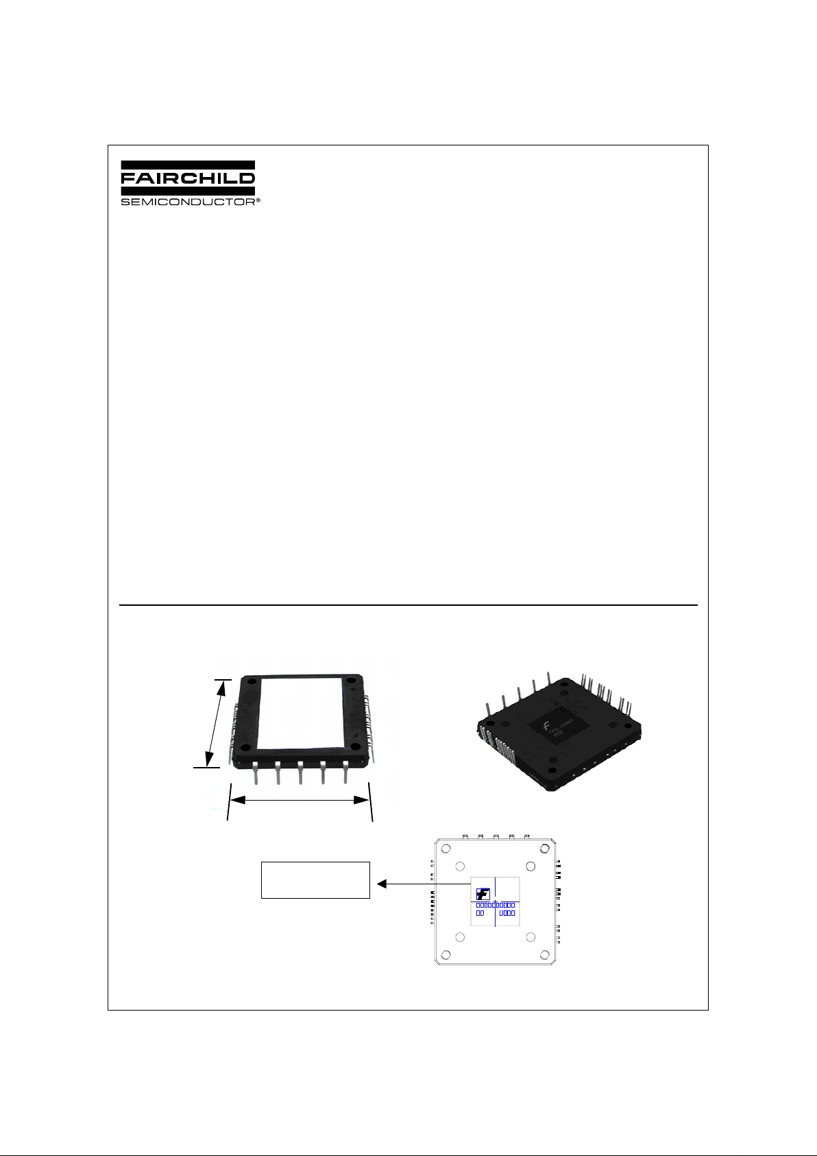
External View and Marking Information
Fig. 1.
55 mm
57 mm
Top View Bottom View
Marking
Device Name
Version, Lot Code
©2002 Fairchild Semiconductor Corporation
FPBL10SH60
Rev. B1, February 2002
Integrated Power Functions
• 600V-10A IGBT inverter for three-phase DC/AC power conversion (Please refer to Fig. 3)
Integrated Drive, Protection and System Control Functions
• For inverter high-side IGBTs: Gate drive circuit, High voltage isolated high-speed level shifting
Control circuit under-voltage (UV) protection
Note) Available bootstrap circuit example is given in Figs. 10, 15 and 16.
• For inverter low-side IGBTs: Gate drive circuit, Short circuit protection (SC)
Control supply circuit under-voltage (UV) protection
• Fault signaling: Corresponding to a SC fault (Low-side IGBTs) or a UV fault (Low-side supply)
• Input interface: 5V CMOS/LSTTL compatible, Schmitt trigger input
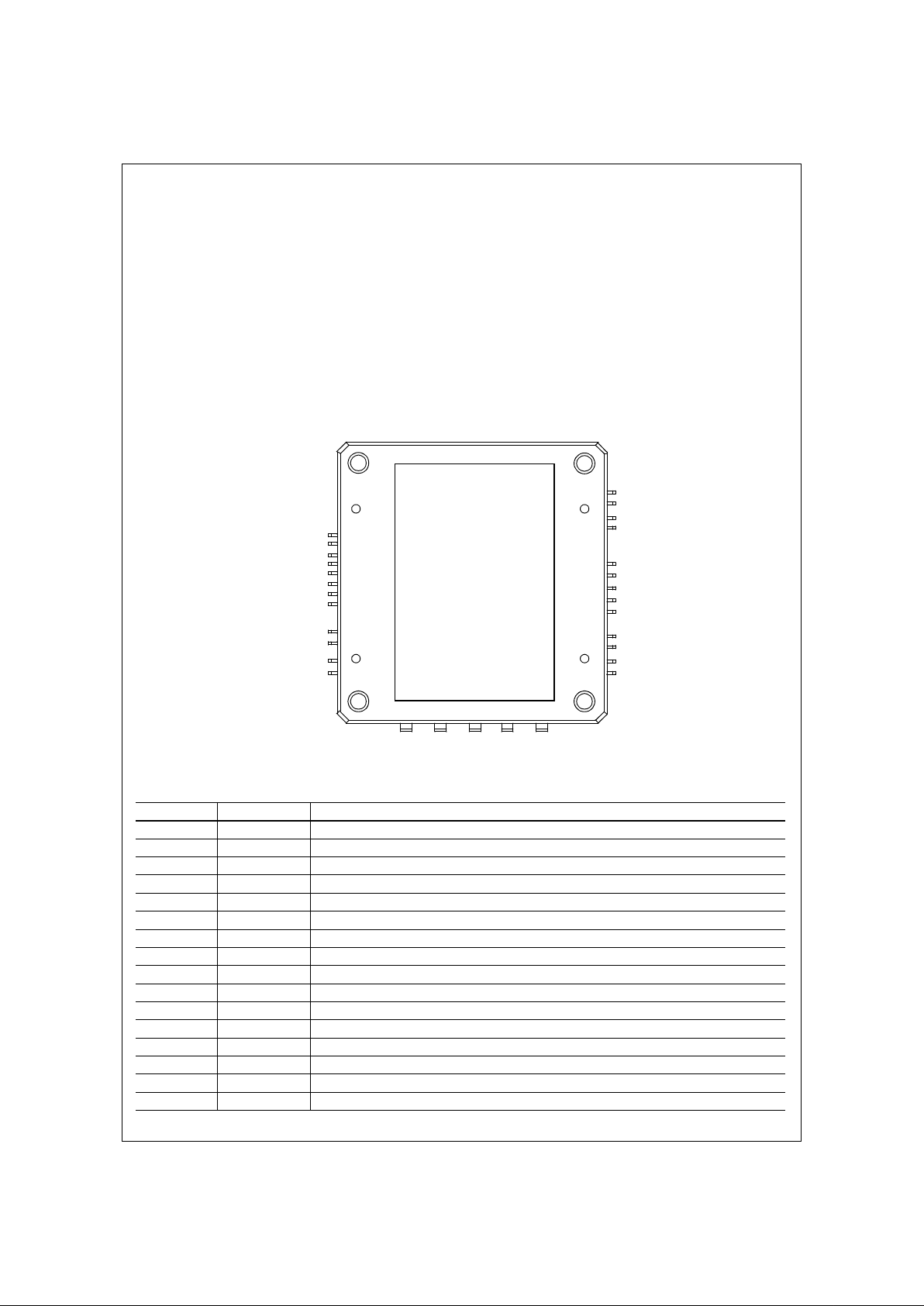
Pin Configuration
Fig. 2.
Pin Descriptions
Pin Number Pin Name Pin Description
1V
CC(L)
Low-side Common Bias Voltage for IC and IGBTs Driving
2COM
(L)
Low-side Common Supply Ground
3IN
(UL)
Signal Input T erminal for Low-side U Phase
4IN
(VL)
Signal Input T erminal for Low-side V Phase
5IN
(WL)
Signal Input T erminal for Low-side W Phase
6V
FO
Fault Output Terminal
7C
FOD
Capacitor for Fault Output Duration Time Selection
8C
SC
Capacitor (Low-pass Filter) for Short-current Detection Input
9R
SC
Resistor for Short-circuit Current Detection
10 NC No Connection
11 NC No Connection
12 NC No Connection
13 W Output Terminal for W Phase
14 V Output Terminal for V Phase
15 U Output Terminal for U Phase
16 N Negative DC–Link Input
V
CC(L)
COM
(L)
IN
(UL)
IN
(VL)
IN
(WL)
V
FO
C
FOD
C
SC
R
SC
NC
NC
NC
WVUNP
V
S(U)
V
B(U)
V
CC(UH)
IN
(UH)
V
S(V)
V
B(V)
V
CC(VH)
IN
(VH)
COM
(H)
V
S(W)
V
B(W)
V
CC(WH)
IN
(WH)
Top View
©2002 Fairchild Semiconductor Corporation
FPBL10SH60
Rev. B1, February 2002
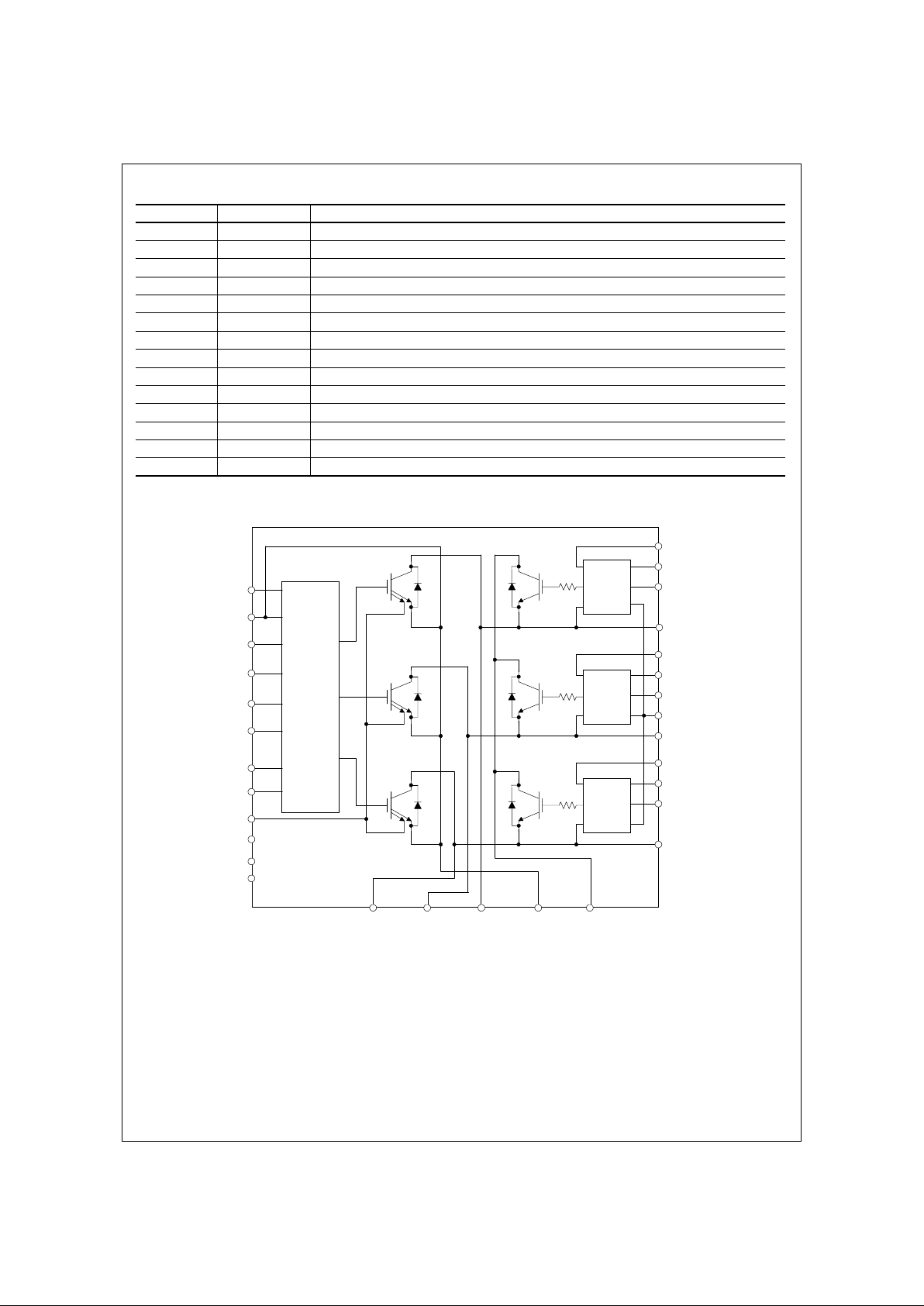
Internal Equivalent Circuit and Input/Output Pins
Note
1. Inverter low-side ( (1) - (12) pins) is composed of three sense-IGBTs including freewheeling diodes for each IGBT and one control IC which has gate driving,
current sensing and protection functions.
2. Inverter power side ( (13) - (17) pins) is composed of two inverter dc-link input terminals and three inverter output terminals.
3. Inverter high-side ( (18) - (30) pins) is composed of three normal-IGBTs including freewheeling diodes and three drive ICs for each IGBT.
Fig. 3.
17 P Positive DC–Link Input
18 IN
(WH)
Signal Input T erminal for High-side W Phase
19 V
CC(WH)
High-side Bias Voltage for W Phase IC
20 V
B(W)
High-side Bias Voltage for W Phase IGBT Driving
21 V
S(W)
High-side Bias Voltage Ground for W Phase IGBT Driving
22 COM
(H)
High-side Common Supply Ground
23 IN
(VH)
Signal Input T erminal for High-side V Phase
24 V
CC(VH)
High-side Bias Voltage for V Phase IC
25 V
B(V)
High-side Bias Voltage for V Phase IGBT Driving
26 V
S(V)
High-side Bias Voltage Ground for V Phase IGBT Driving
27 IN
(UH)
Signal Input T erminal for High-side U Phase
28 V
CC(UH)
High-side Bias Voltage for U Phase IC
29 V
B(U)
High-side Bias Voltage for U Phase IGBT Driving
30 V
S(U)
High-side Bias Voltage Ground for U Phase IGBT Driving
Pin Descriptions (Continued)
Pin Number Pin Name Pin Description
WVUN
(14) (15) (16)
(17)
P
(1) V
CC(L)
(2) COM
(L)
(3) IN
(UL)
(4) IN
(VL)
(5) IN
(WL)
(6) V
FO
(7) C
FOD
(8) C
SC
(12) NC
(11) NC
(13)
(29) V
B(U)
(22) COM
(H)
(27) IN
(UH)
(30) V
S(U)
(28) V
CC(UH)
(25) V
B(V)
(23) IN
(VH)
(24) V
CC(VH)
(26) V
S(V)
(20) V
B(W)
(18) IN
(WH)
(19) V
CC(WH)
(21) V
S(W)
(10) NC
(9) R
SC
V
CC
Wout
Uout
Vout
C
(SC)
C
(FOD)
V
(FO)
IN
(WL)
IN
(VL)
IN
(UL)
COM
(L)
Vcc
IN
COM
VB
HO
VS
Vcc
IN
COM
VB
HO
VS
Vcc
IN
COM
VB
HO
VS
©2002 Fairchild Semiconductor Corporation
FPBL10SH60
Rev. B1, February 2002
Absolute Maximum Ratings
Inverter Part
(TC = 25°C, Unless Otherwise Specified)
Note
1. It would be recommended that the average junction temperature should be limited to TJ ≤ 125°C (@TC ≤ 100°C) in order to guarantee safe operation.
Control Part
(TC = 25°C, Unless Otherwise Specified)
Total System
Item Symbol Condition Rating Unit
Supply Voltage V
DC
Applied to DC - Link 450 V
Supply Voltage (Surge) V
PN(Surge)
Applied between P- N 500 V
Collector-Emitter Voltage V
CES
600 V
Each IGBT Collector Current ± I
C
TC = 25°C (Note Fig. 4) 10 A
Each IGBT Collector Current (Peak) ± I
CP
TC = 25°C (Note Fig. 4) 20 A
Collector Dissipation P
C
TC = 25°C per One Chip 43 W
Operating Junction Temperature T
J
(Note 1) -55 ~ 150 °C
Item Symbol Condition Rating Unit
Control Supply Voltage V
CC
Applied between V
CC(H)
- COM
(H)
, V
CC(L)
- COM
(L)
18 V
High-side Control Bias Voltage V
BS
Applied between V
B(U)
- V
S(U)
, V
B(V)
- V
S(V)
, V
B(W)
-
V
S(W)
20 V
Input Signal Voltage V
IN
Applied between IN
(UH)
, IN
(VH)
, IN
(WH)
- COM
(H)
IN
(UL)
, IN
(VL)
, IN
(WL)
- COM
(L)
-0.3 ~ 6.0 V
Fault Output Supply Voltage V
FO
Applied between VFO - COM
(L)
-0.3~VCC+0.5 V
Fault Output Current I
FO
Sink Current at VFO Pin 5 mA
Current Sensing Input Voltage V
SC
Applied between CSC - COM
(L)
-0.3~VCC+0.5 V
Item Symbol Condition Rating Unit
Self Protection Supply Voltage Limit
(Short Circuit Protection Capability)
V
DC(PROT)
Applied to DC - Link,
V
CC
= VBS = 13.5 ~ 16.5V
T
J
= 125°C, Non-repetitive, less than 6µs
400 V
Module Case Operation Temperature T
C
Note Fig. 4 -20 ~ 100 °C
Storage Temperature T
STG
-55 ~ 150 °C
Isolation Voltage V
ISO
60Hz, Sinusoidal, AC 1 minute, Connection
Pins to Heat-sink Plate
2500 V
rms
©2002 Fairchild Semiconductor Corporation
FPBL10SH60
Rev. B1, February 2002
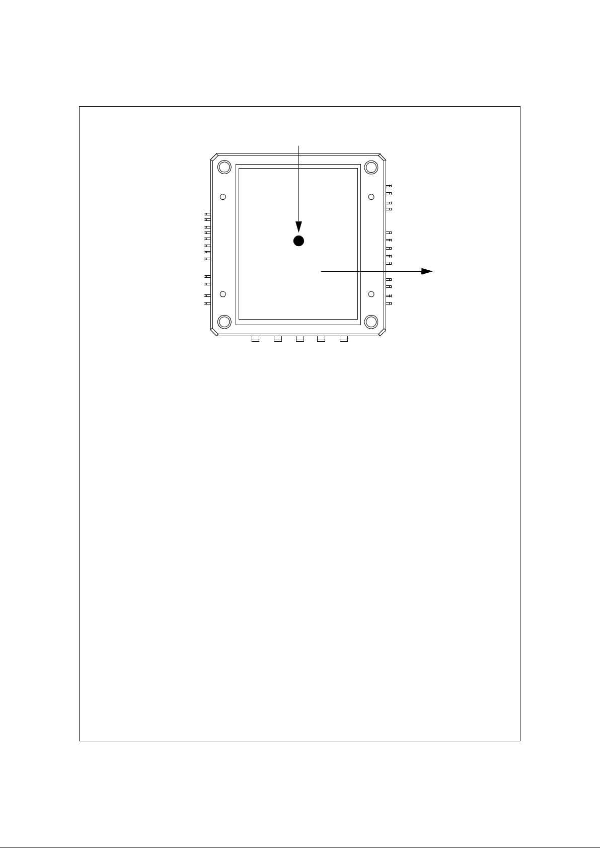
Fig. 4. Tc Measurement Point
V
CC(L)
COM
(L)
IN
(UL)
IN
(VL)
IN
(WL)
V
FO
C
FOD
C
SC
R
SC
NC
NC
NC
WVUNP
V
S(U)
V
B(U)
V
CC(UH)
IN
(UH)
V
S(V)
V
B(V)
V
CC(VH)
IN
(VH)
COM
(H)
V
S(W)
V
B(W)
V
CC(WH)
IN
(WH)
Case Temperature (TC) Detecting Point
Ceramic
Substate

©2002 Fairchild Semiconductor Corporation
FPBL10SH60
Rev. B1, February 2002
Absolute Maximum Ratings
Thermal Resistance
Note
2. For the measurement point of case temperature (Tc), please refer to Fig. 4.
Electrical Characteristics
Inverter Part
(Tj = 25°C, Unless Otherwise Specified)
Note
3. tON and t
OFF
include the propagation del ay time of th e internal drive IC. t
C(ON)
and t
C(OFF)
are the switching time o f IGBT itself u nder the given gate drivin g condition
internally. For the detailed information, please see Fig. 5.
Item Symbol Condition Min. Typ. Max. Unit
Junction to Case Thermal
Resistance
R
th(j-c)Q
Each IGBT under Inverter Operating Condition
(Note 2)
- - 2.89 °C/W
R
th(j-c)F
Each FWDi under Inverter Operating Condition
(Note 2)
- - 3.73 °C/W
Contact Thermal
Resistance
R
th(c-f)
Ceramic Substrate (per 1 Module)
Thermal Grease Applied
- - 0.06 °C/W
Item Symbol Condition Min. Typ. Max. Unit
Collector - Emitter
Saturation Voltage
V
CE(SAT)VCC
= VBS = 15V
V
IN
= 0V
I
C
= 10A, Tj = 25°C - - 2.8 V
I
C
= 10A, Tj = 125°C - - 2.9 V
FWDi Forward Voltage V
FMVIN
= 5V IC = 10A, Tj = 25°C - - 2.3 V
I
C
= 10A, Tj = 125°C - - 2.1 V
Switching Times t
ON
VPN = 300V, VCC = VBS = 15V
I
C
= 10A, Tj = 25°C
V
IN
= 5V ↔ 0V, Inductive Load
(High-Low Side)
(Note 3)
-0.37- µs
t
C(ON)
-0.12- µs
t
OFF
-0.53- µs
t
C(OFF)
-0.2-µs
t
rr
-0.1-µs
Collector - Emitter
Leakage Current
I
CESVCE
= V
CES
, Tj = 25°C - - 250 µA
 Loading...