

Fairchild Semiconductor FM24C32U Datasheet
FM24C32U – 32K-Bit Standard 2-Wire Bus
Interface Serial EEPROM
FM24C32U – 32K-Bit Standard 2-Wire Bus Interface Serial EEPROM
September 2002
General Description
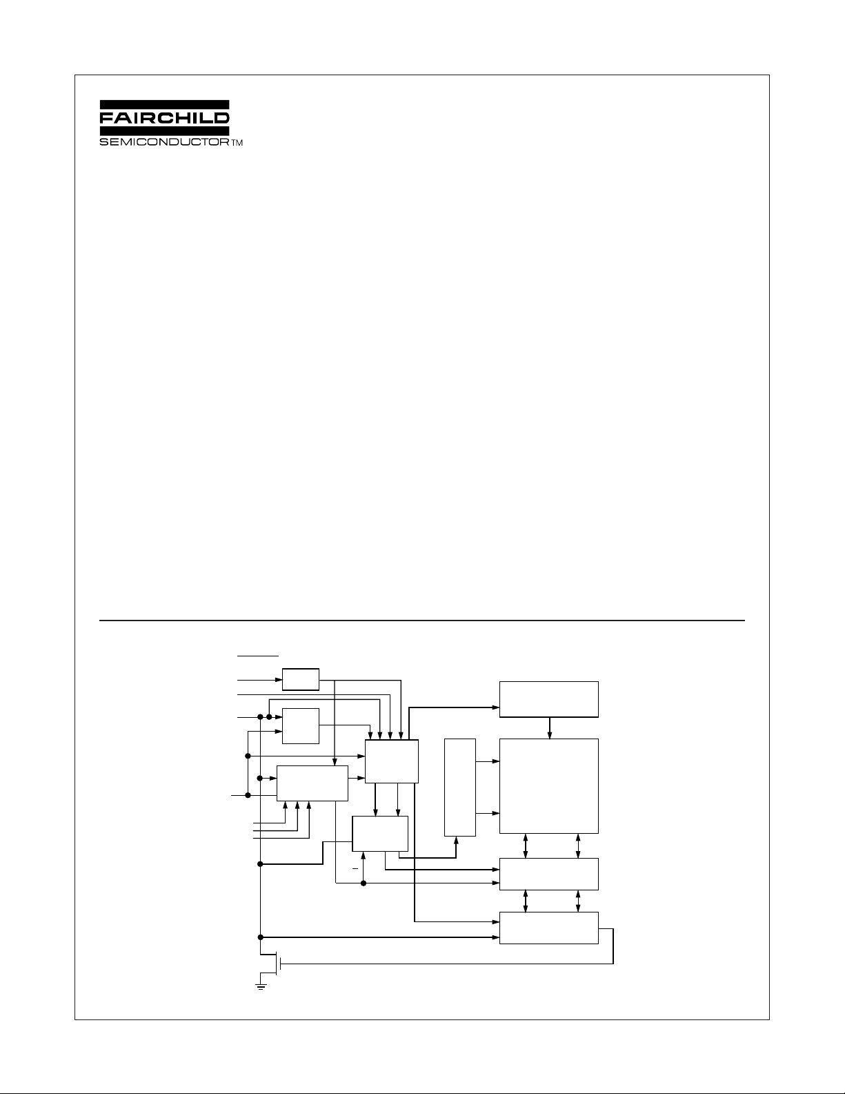
FM24C32U is a 32Kbit CMOS non-volatile serial EEPROM organized as 4K x 8 bit memory. This device confirms to Extended IIC
2-wire protocol that allows accessing of memory in excess of
16Kbit on an IIC bus. This serial communication protocol uses a
Clock signal (SCL) and a Data signal (SDA) to synchronously
clock data between a master (e.g. a microcontroller) and a slave
(EEPROM). FM24C32U is designed to minimize pin count and
simplify PC board layout requirements.
FM24C32U offers hardware write protection where by the upper
half (upper 16Kbit) of the memory array can be write protected by
connecting WP pin to VCC. This section of memory then becomes
unalterable until the WP pin is switched to VSS.
“LZ” and “L” versions of FM24C32U offer very low standby current
making them suitable for low power applications. This device is
offered in both SO and DIP packages.
Fairchild EEPROMs are designed and tested for applications
requiring high endurance, high reliability and low power consumption.
Block Diagram
V
SS
V
SDA
CC
WP
WRITE
LOCKOUT
START
STOP
LOGIC
Features
■ Extended operating voltage: 2.7V to 5.5V
■ Up to 400 KHz clock frequency at 2.7V to 5.5V
■ Low power consumption
— 0.2mA active current typical
—10µA standby current typical
—1µA standby current typical (L version)
— 0.1µA standby current typical (LZ version)
■ Schmitt trigger inputs
■ 32 byte page write mode
■ Self timed write cycle (6ms typical)
■ Hardware Write Protection for upper half of the array
■ Low VCC programming lockout for VCC = 5V±10% (“H” option)
— Internal ERASE/WRITE logic is disabled if VCC is below 3.8V
■ Endurance: 1 Million data changes
■ Data Retention: Greater than 40 years
■ Packages: 8-Pin DIP and 8-Pin SO
■ Temperature range
— Commercial: 0°C to +70°C
— Industrial (V): -40°C to +85°C
— Automotive (E): -40°C to +125°C
H.V. GENERATION
TIMING &CONTROL
SCL
A2
A1
A0
© 2001 Fairchild Semiconductor Corporation
FM24C32U Rev. A.1
SLAVE ADDRESS
REGISTER &
COMPARATOR
R/W
CONTROL
LOGIC
WORD
ADDRESS
COUNTER
D
IN
E2PROM
XDEC
CK
1
ARRAY
YDEC
DATA REGISTER
D
OUT
www.fairchildsemi.com
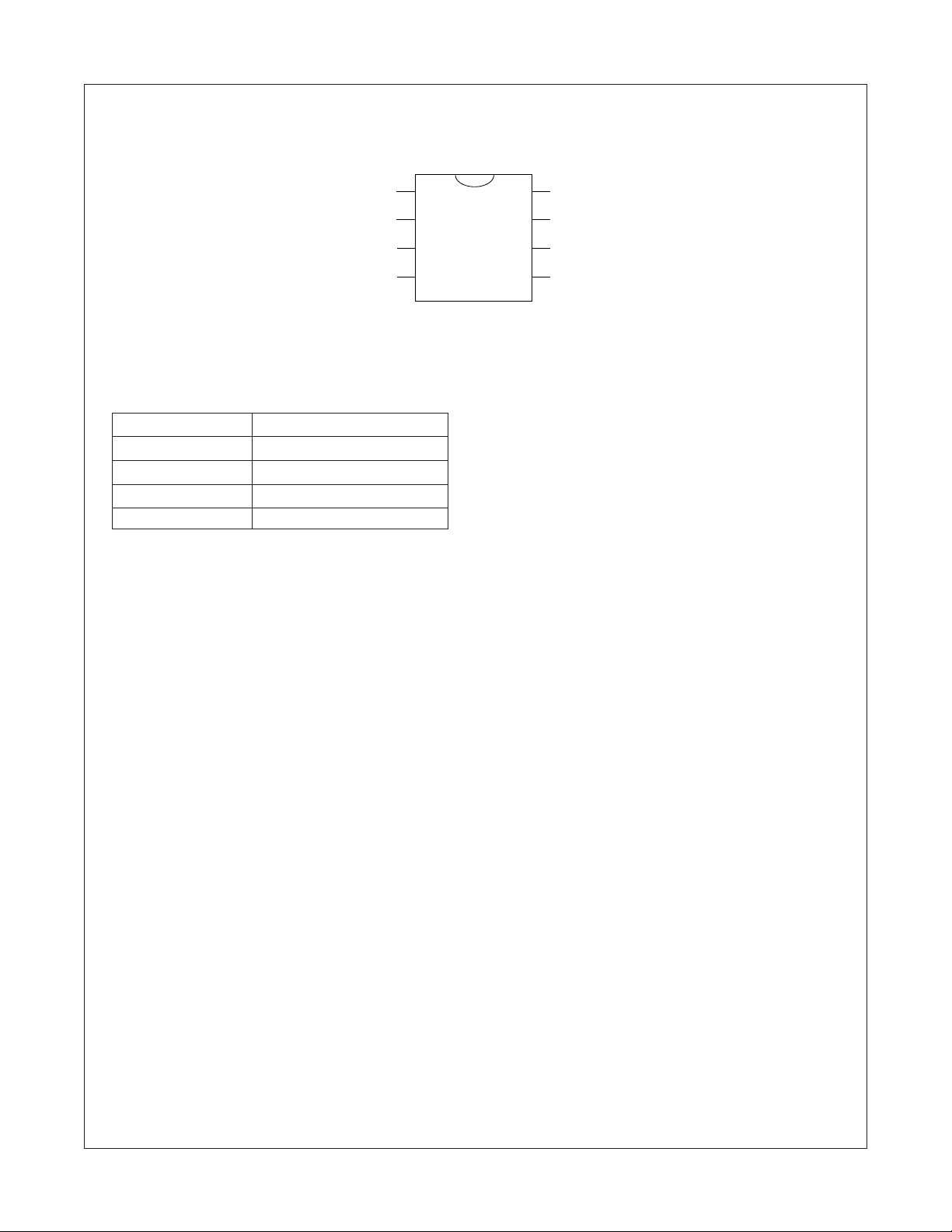
Connection Diagram
FM24C32U – 32K-Bit Standard 2-Wire Bus Interface Serial EEPROM
Dual-in-Line Package (N) and SO Package (M8)
Pin Names
V
SS
SDA Serial Data I/O
SCL Serial Clock Input
WP Write Protect
V
CC
See Package Number N08E and M08A
Ground
Power Supply
A0
1
A1
2
A2
V
SS
FM24C32U
3
4
V
8
CC
WP
7
SCL
6
SDA
5
FM24C32U Rev. A.1
2
www.fairchildsemi.com
Ordering Information
FM 24 C XX U F T LZ E XXX Letter Description
FM24C32U – 32K-Bit Standard 2-Wire Bus Interface Serial EEPROM
Package N 8-pin DIP
M8 8-pin SOIC
Temp. Range None 0 to 70°C
V -40 to +125°C
E -40 to +85°C
Voltage Operating Range Blank 4.5V to 5.5V
H 4.5V to 5.5V and V
Lockout
L 2.7V to 5.5V
LZ 2.7V to 5.5V and
<1µA Standby Current
Blank Normal Pin Out
T Rotated Die Pin Out
SCL Clock Frequency Blank 100KHz
F 400KHz
Process U Ultralite Process
Density 32 32K with Write Protect
CC
C CMOS Technology
Interface 24 IIC
FM Fairchild Non-Volatile
Memory
FM24C32U Rev. A.1
3
www.fairchildsemi.com
Product Specifications
FM24C32U – 32K-Bit Standard 2-Wire Bus Interface Serial EEPROM
Absolute Maximum Ratings
Ambient Storage Temperature –65°C to +150°C
All Input or Output Voltages
with Respect to Ground 6.5V to –0.3V
Lead Temperature
(Soldering, 10 seconds) +300°C
ESD Rating 2000V min.
Operating Conditions
Ambient Operating Temperature
FM24C32U 0°C to +70°C
FM24C32UE -40°C to +85°C
FM24C32UV -40°C to +125°C
Positive Power Supply
FM24C32U/FM24C32UH 4.5V to 5.5V
FM24C32UL 2.7V to 5.5V
FM24C32ULZ 2.7V to 5.5V
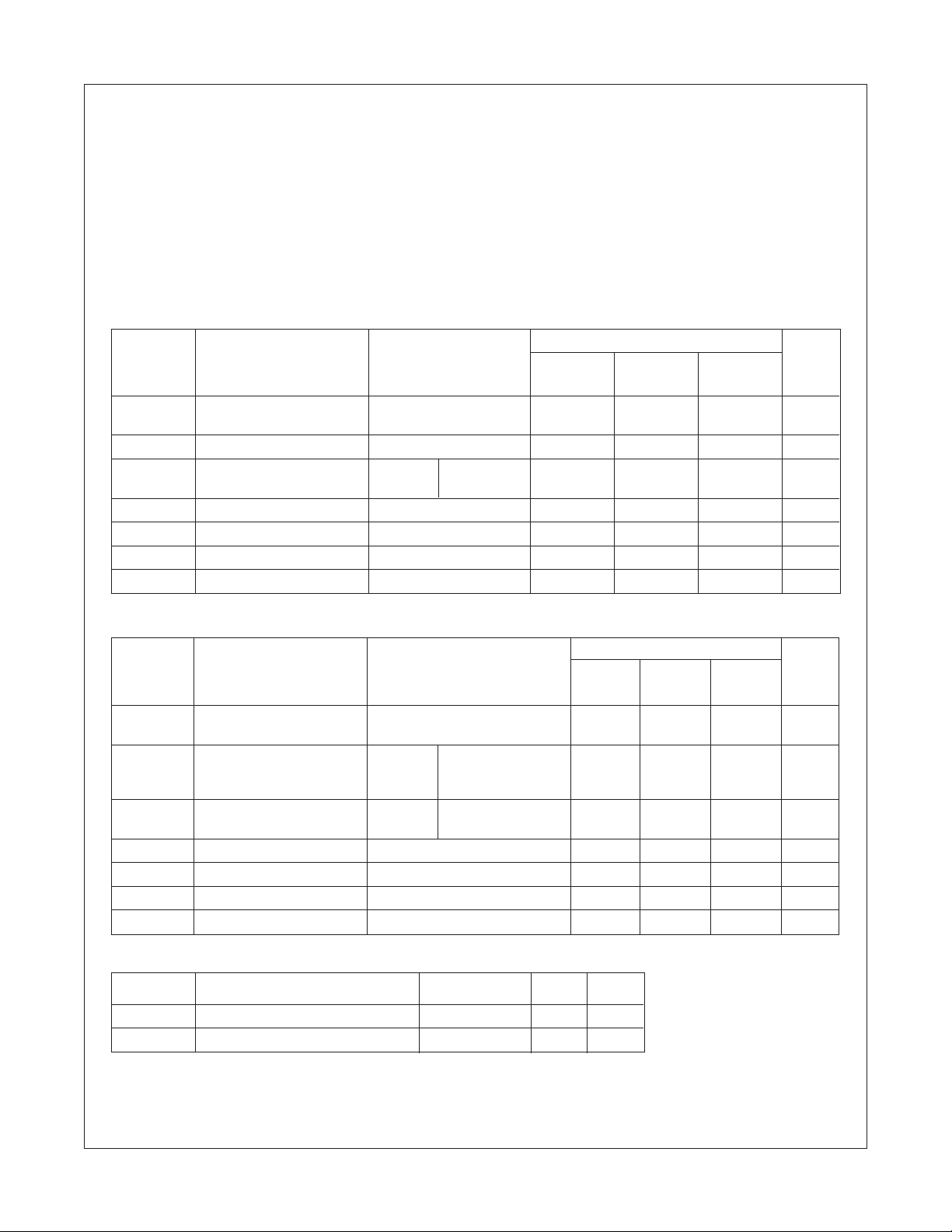
Standard VCC (4.5V to 5.5V) DC Electrical Characteristics
Symbol Parameter Test Conditions Limits Units
Min Typ Max
(Note 1)
I
V
V
CCA
I
SB
I
LI
I
LO
V
OL
IL
IH
Active Power Supply f
Current f
Standby Current VIN = GND or V
= 400 KHz 0.2 1.0 mA
SCL
= 100 KHz
SCL
CC
10 50 µA
Input Leakage Current VIN = GND A0, A1, A2, WP 0.1 1 µA
Output Leakage Current V
to V
OUT
CC
SCL 0.5 2 µA
= GND to V
CC
0.1 1 µA
Input Low Voltage –0.3 VCC x 0.3 V
Input High Voltage VCC x 0.7 VCC + 0.5 V
Output Low Voltage I
= 3 mA 0.4 V
OL
Low VCC (2.7V to 5 .5V) DC Electrical Characteristics
Symbol Parameter Test Conditions Limits Units
Min Typ Max
(Note 1)
I
CCA
I
SB
(Note 3) or V
I
LI
I
LO
V
IL
V
IH
V
OL
Capacitance T
Symbol Test Conditions Max Units
C
I/O
C
IN
Note 1: Typical values are TA = 25°C and nominal supply voltage (5V).
Note 2: This parameter is periodically sampled and not 100% tested.
Note 3: The "L" and "LZ" versions can be operated in the 2.7V to 5.5V VCC range. However the ISB values for L and LZ are applicable only when VCC is in the 2.7V to 4.5V range.
Active Power Supply Current f
= 400 KHz 0.2 1.0 mA
SCL
f
= 100 KHz
SCL
Standby Current VIN = GND VCC = 2.7V - 4.5V (L) 1 10 µA
CC
VCC = 2.7V - 4.5V (LZ) 0.1 1 µA
VCC = 4.5V - 5.5V 10 50 µA
Input Leakage Current VIN = GND A0, A1, A2, WP 0.1 1 µA
to V
CC
Output Leakage Current V
= GND to V
OUT
Input Low Voltage –0.3 V
SCL 0.5 2 µA
CC
0.1 1 µA
x 0.3 V
CC
Input High Voltage VCC x 0.7 VCC + 0.5 V
Output Low Voltage IOL = 3 mA 0.4 V
= +25°C, f = 100/400 KHz, VCC = 5V (Note 2)
A
Input/Output Capacitance (SDA) V
= 0V 8 pF
I/O
Input Capacitance (A0, A1, A2, SCL) VIN = 0V 6 pF
FM24C32U Rev. A.1
4
www.fairchildsemi.com
 Loading...