

Fairchild Semiconductor FM24C256N Datasheet
1
www.fairchildsemi.com
FM24C256 rev. B.3
FM24C256 256 KBit 2-Wire Bus Interface Serial EEPROM with Write Protect
June 2000
© 2000 Fairchild Semiconductor International
FM24C256
256 KBit 2-Wire Bus Interface
Serial EEPROM with Write Protect
General Description
The FM24C256/C256L/C256LZ devices are 256 Kbits CMOS
nonvolatile electrically erasable memory. These devices offer the
designer different low voltage and low power options. They
conform to all requirements in the Extended IIC 2-wire protocol.
Furthermore, they are designed to minimize device pin count and
simplify PC board layout requirements.
The entire memory array can be write disabled (Write Protection)
by connecting the WP pin to VCC.
Functional address lines allow up to eight devices on the same
bus, for up to a total of 2 Mbit address space.
The IIC communication protocol uses CLOCK (SCL) and DATA
I/O (SDA) lines to synchronously clock data between the master
(for example a microprocessor) and the slave EEPROM device(s).
Fairchild EEPROMs are designed and tested for applications
requiring high endurance, high reliability, and low power consumption.
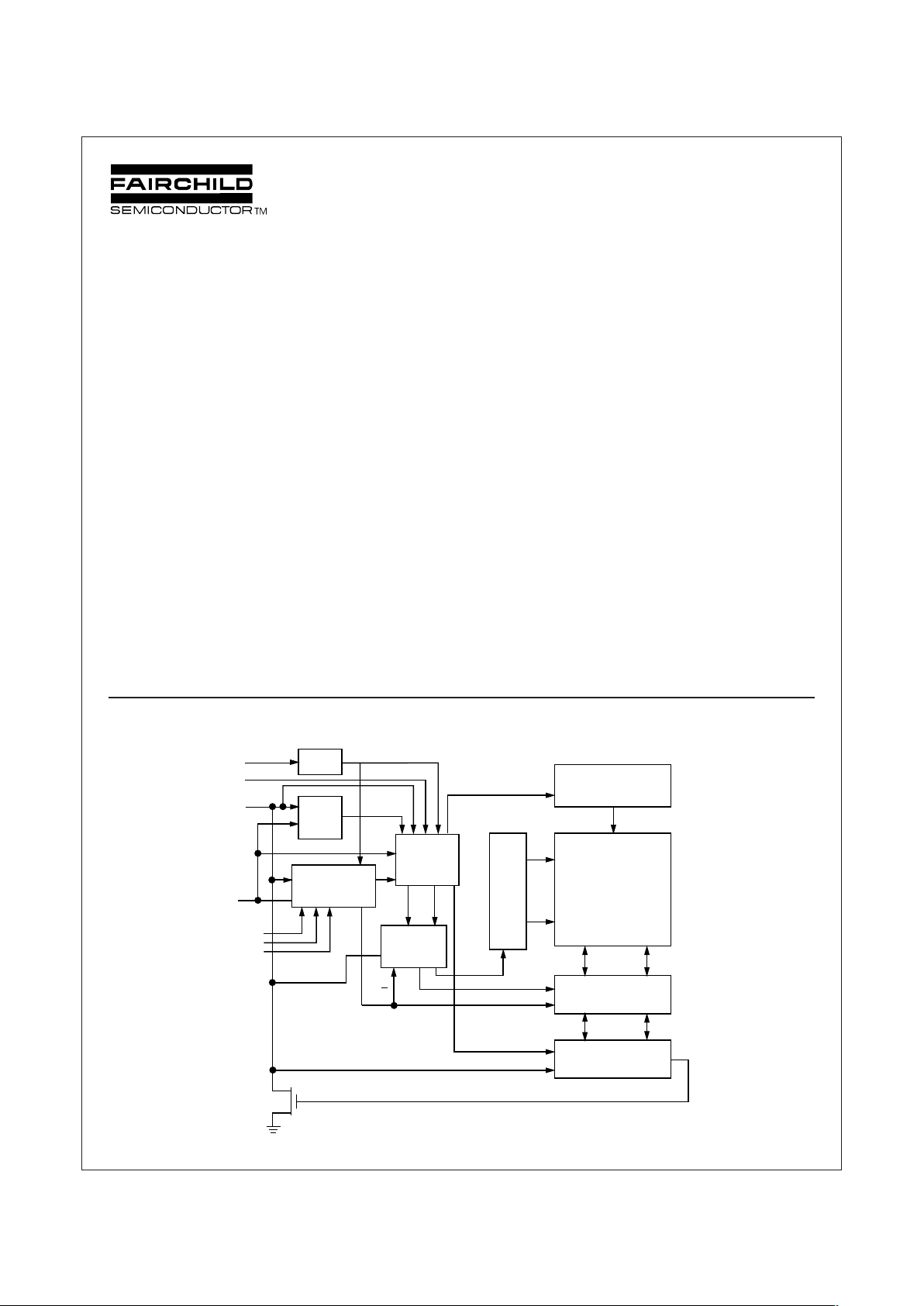
Block Diagram
Features
■ Extended Operating Voltages
— C256: 4.5V - 5.5V
— C256L: 2.7V - 5.5V
— C256LZ: 2.7V - 5.5V
■ Low Power CMOS
— 1mA active current typical
— C256/C256L: 10µA standby current typical
— C256LZ: less than 1µA standby current
■ 2-wire IIC serial interface
■ 64 byte page write mode
■ Max write cycle time of 6ms byte/page
■ 40 years data retention
■ Endurance: 100,000 data changes
■ Hardware write protect for entire array
■ Schmitt trigger inputs for noise suppression
■ Electrostatic discharge protection > 4000V
■ 8-pin DIP and 8-pin SO (150 mil) packages. Contact factory
for CSP package availability
DS800023-1
H.V. GENERATION
TIMING &CONTROL
E2PROM
ARRAY
YDEC
DATA REGISTER
XDEC
CONTROL
LOGIC
WORD
ADDRESS
COUNTER
SLAVE ADDRESS
REGISTER &
COMPARATOR
START
STOP
LOGIC
WRITE
LOCKOUT
START CYCLE
CK
D
IN
R/W
LOAD INC
SDA
SCL
WP
V
CC
D
OUT
A2
A1
A0
2
www.fairchildsemi.com
FM24C256 rev. B.3
FM24C256 256 KBit 2-Wire Bus Interface Serial EEPROM with Write Protect
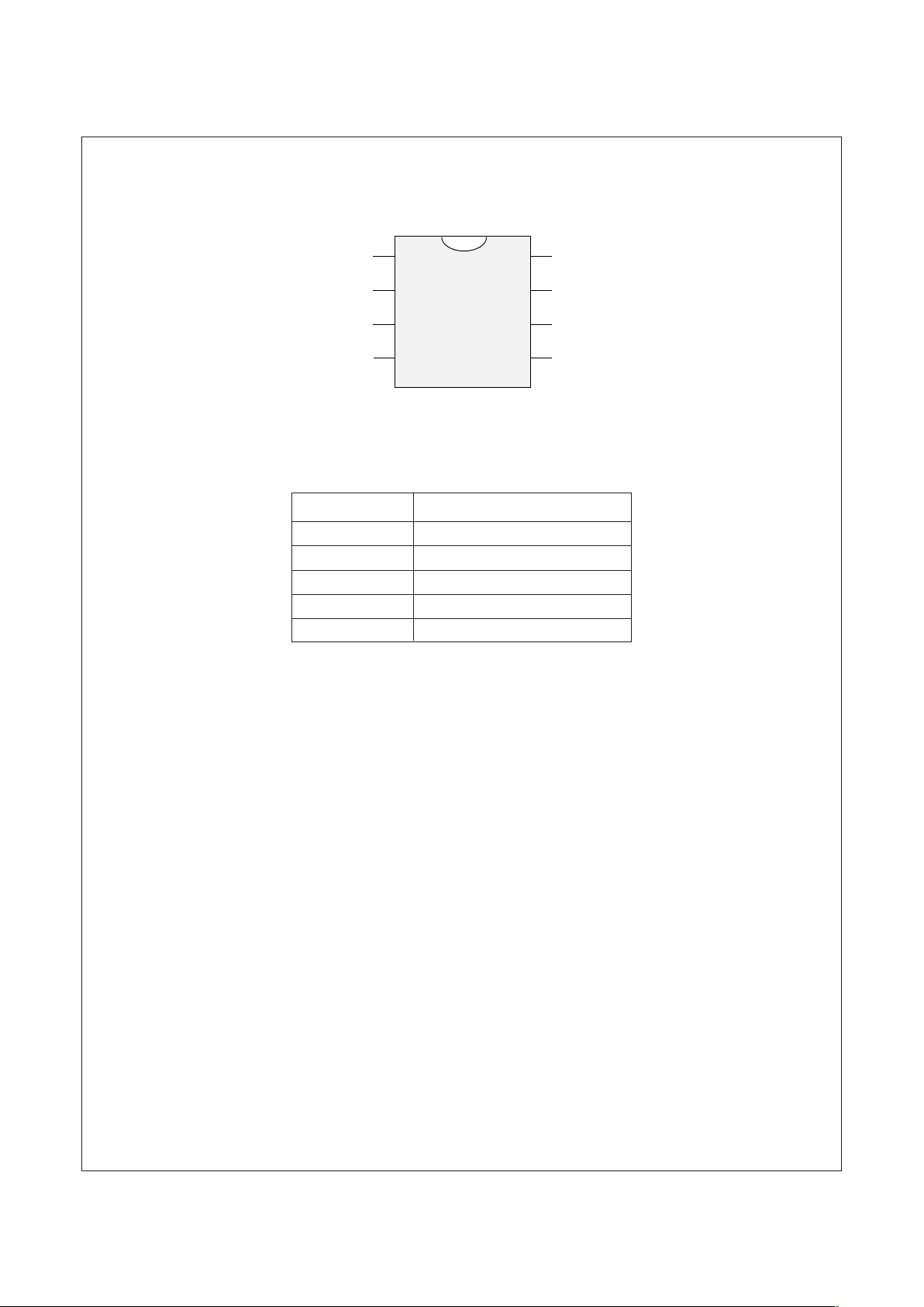
Connection Diagram
Dual-In-Line Package (N)
and 8-Pin SO Package (M8)
Top View
See Package Number N08E and M08A
Pin Names
A0, A1, A2 Device Address Input
V
SS
Ground
SDA Data I/O
SCL Clock Input
WP Write Protect
V
CC
Power Supply
A0
A1
A2
V
SS
V
CC
WP
SCL
SDA
8
7
6
5
1
2
3
4
FM24C256
DS800023-2

3
www.fairchildsemi.com
FM24C256 rev. B.3
FM24C256 256 KBit 2-Wire Bus Interface Serial EEPROM with Write Protect
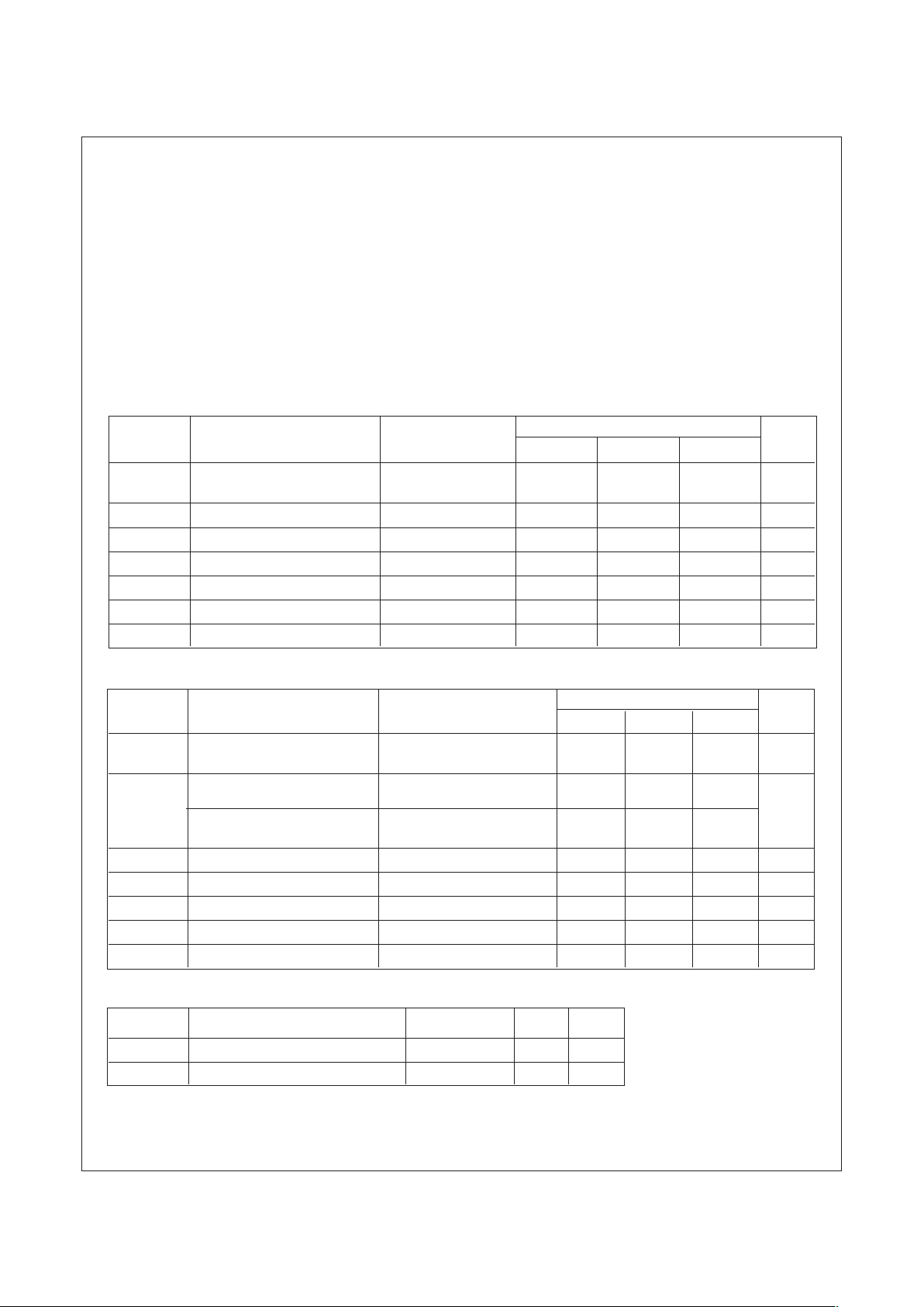
Ordering Information
FM 24 C XX F LZ E YY X Letter Description
Blank Tube
X Tape and Reel
Package N 8-pin DIP
M8 8-pin SO8
Temp. Range Blank 0 to 70°C
E -40 to +85°C
Voltage Operating Range Blank 4.5V to 5.5V
L 2.7V to 5.5V
LZ 2.7V to 5.5V and
<1µA Standby Current
SCL Clock Frequency Blank 100KHz
F 400KHz
Density 256 256K with write protect
C CMOS
Interface 24 IIC - 2 Wire
FM Fairchild Non-Volatile
Memory
Part Number Clock Frequency V
CC
Standby Current
FM24C256YYX 4.5V - 5.5V 10µA typical
FM24C256LYYX 100KHz 2.7V - 5.5V
FM24C256LZYYX 1µA max
FM24C256FYYX 4.5V - 5.5V 10µA typical
FM24C256FLYYX 400KHz 2.7V - 5.5V
FM24C256FLZYYX 1µA max
Part Number Clock Frequency V
CC
Standby Current
FM24C256EYYX 4.5V - 5.5V 10µA typical
FM24C256LEYYX 100KHz 2.7V - 5.5V
FM24C256LZEYYX 1µA max
FM24C256FEYYX 4.5V - 5.5V 10µA typical
FM24C256FLEYYX 400KHz 2.7V - 5.5V
FM24C256FLZEYYX 1µA max
Commercial Temperature Range: 0° to +70°C
Industrial Temperature Range: -40° to +85°C
4
www.fairchildsemi.com
FM24C256 rev. B.3
FM24C256 256 KBit 2-Wire Bus Interface Serial EEPROM with Write Protect
Absolute Maximum Ratings
Ambient Storage Temperature –65°C to +150°C
All Input or Output Voltages
with Respect to Ground 6.5V to –0.3V
Lead Temperature
(Soldering, 10 seconds) +300°C
ESD Rating 4000V min.
Operating Conditions
Ambient Operating Temperature
FM24C256/L/LZ 0°C to +70°C
FM24C256F/FL/FLZ 0°C to +70°C
FM24C256E/LE/LZE -40°C to +85°C
FM24C256FE/FLE/FLZE -40°C to +85°C
Positive Power Supply
FM24C256/E 4.5V to 5.5V
FM24C256F/FE 4.5V to 5.5V
FM24C256L/LZ 2.7V to 5.5V
FM24C256FL/FLZ 2.7V to 5.5V
FM24C256LE/LZE 2.7V to 5.5V
FM24C256FLE/FLZE 2.7V to 4.5V
Standard VCC (4.5V to 5.5V) DC Electrical Characteristics
Symbol Parameter Test Conditions Limits Units
Min Typ Max
I
CCA
Active Power Supply Current f
SCL
= 100 kHz 0.5 1.0 mA
f
SCL
= 400 kHz
I
SB
Standby Current VIN = GND or V
CC
10 50 µA
I
LI
Input Leakage Current VIN = GND to V
CC
0.1 1 µA
I
LO
Output Leakage Current V
OUT
= GND to V
CC
0.1 1 µA
V
IL
Input Low Voltage –0.3 VCC x 0.3 V
V
IH
Input High Voltage VCC x 0.7 VCC + 0.5 V
V
OL
Output Low Voltage I
OL
= 2.1 mA 0.4 V
Low VCC (2.7V to 5.5V) DC Electrical Characteristics
Symbol Parameter Test Conditions Limits Units
Min Typ Max
I
CCA
Active Power Supply Current f
SCL
= 100 kHz 0.5 1.0 mA
f
SCL
= 400 kHz
I
SB
Standby Current for L VIN = GND or VCC = 4.5V - 5.5V 10 50 µA
(Note 1) VIN = GND or VCC = 2.7V - 4.5V 1 10
Standby Current for LZ VIN = GND or VCC = 4.5V - 5.5V 10 50
VIN = GND or VCC = 2.7V - 4.5V 0.1 1
I
LI
Input Leakage Current VIN = GND to V
CC
0.1 1 µA
I
LO
Output Leakage Current V
OUT
= GND to V
CC
0.1 1 µA
V
IL
Input Low Voltage –0.3 V
CC
x 0.3 V
V
IH
Input High Voltage VCC x 0.7 VCC + 0.5 V
V
OL
Output Low Voltage IOL = 2.1 mA 0.4 V
Capacitance T
A
= +25°C, f = 100/400 KHz, VCC = 5V
Symbol Test Conditions Max Units
C
I/O
Input/Output Capacitance (SDA) V
I/O
= 0V 8 pF
C
IN
Input Capacitance (A0, A1, A2, SCL) VIN = 0V 6 pF
Note 1: Typical values are for TA = 25°C and nominal supply voltage (5V).
 Loading...