

Fairchild Semiconductor FM20 Datasheet
www.fairchildsemi.com
FM20
Ultra-Low-Power Analog Temperature Sensor
Features
• Analog Output, -11.77mV/°C
• Range, -55 to 130°C
• Accuracy, ±1°C at 25°C
• Supply Current, 9µA typical
• Output Drive, 1µA
• Self-heating < 0.021°C
• Operating Voltage: +2.4V to +6V
Applications
• Mobile Phones
• Computers
• Battery Management
• Office Equipment
•HVAC
• Power Supply Modules
• Disk Drives
• Automotive
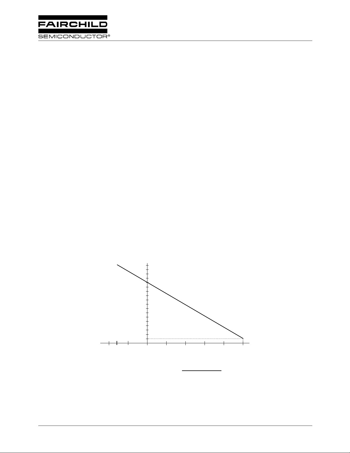
Thermal Response
Description
As a precision CMOS temperature sensor, the FM20 is
cost-effective for accurate low-power temperature
monitoring applications. Output voltage versus temperature
is extremely linear. With no load, the supply current is
typically 1µA. For normal operation, the load on V
should be 5M Ω or less.
In a typical application, a remotely mounted FM20 is
monitored by a microcontroller with an analog A/D
converter input. Alternatively, the FM20 can drive a
comparator with a high impedance input.
Accuracy is typically ±1°C at room temperature; and better
than ±2.5°C from 0 to 50°C.
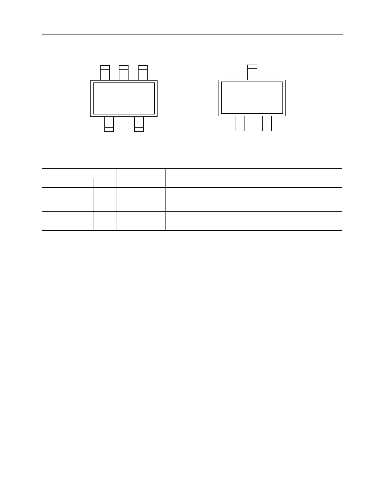
Available packages are surface mount 5-pin SC70 and 3-pin
SOT-23.
V
(mV)
OUT
OUT
1863.9
391
25 50 75 100 125-25-50 -40 0
Temperature (˚C)
V
– 1863.9mV
Temperature (˚C) =
FM20 Output Voltage vs. Temperature
OUT
–11.77mV/˚C
REV. 1.0.6 1/9/03
FM20 PRODUCT SPECIFICATION
Pin Assignments
VOUT
GND
321
FM20
DD GND
V
Pin Descriptions
Pin No.
Pin Name
V
OUT
V
DD
GND 2, 5 3 Power
3 2 Analog Output Temperature Sense. Analog output voltage indicating
41 Power Supply Voltage. 2.4 to 6.0V
Type FunctionSC-70 SOT-23
N/C
54
temperature.
V
= 1863.9 – 11.77 T(°C) mV
OUT
Ground.
GND
3
FM20
12
VDD
VOUT
2
REV. 1.0.6 1/9/03
≤
≤
PRODUCT SPECIFICATION FM20
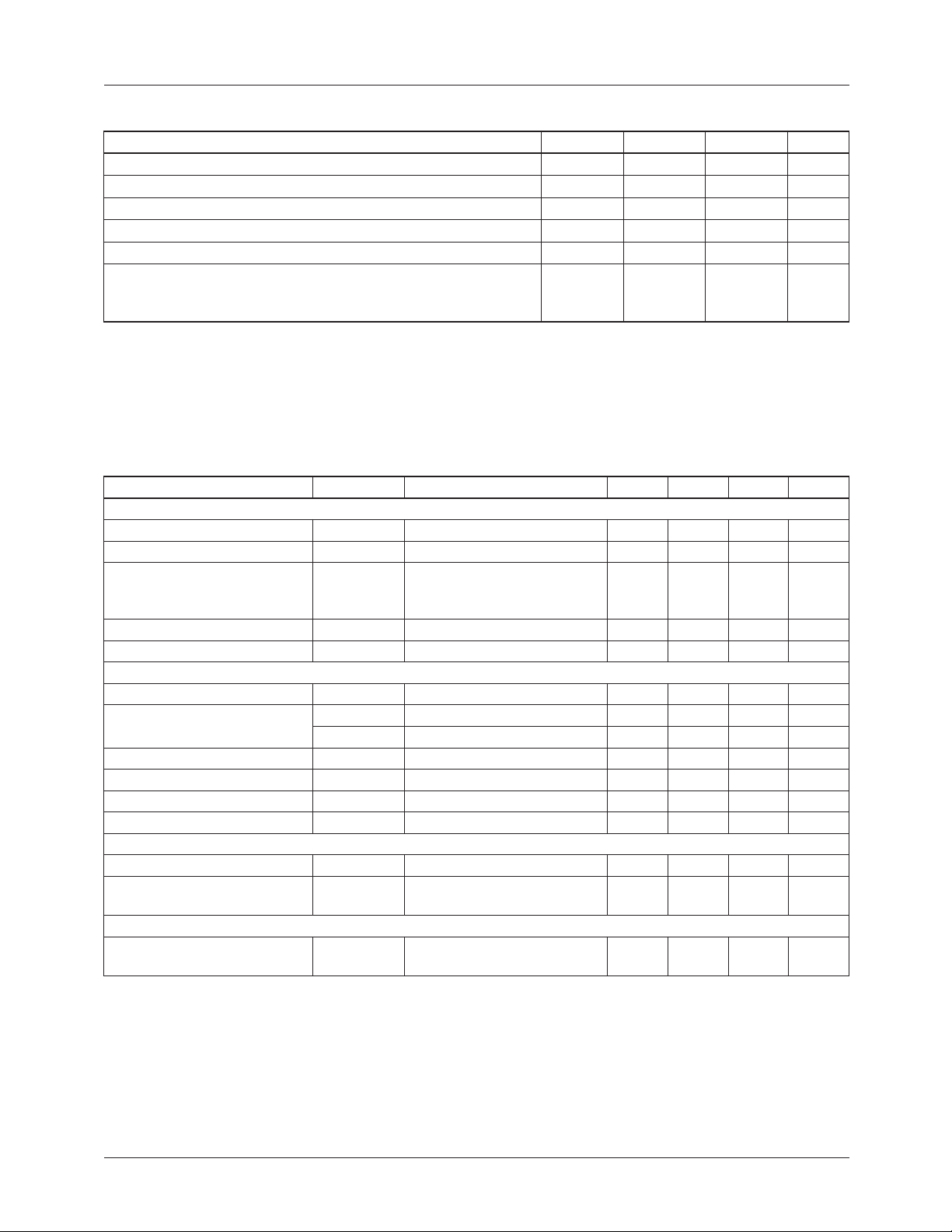
Absolute Maximum Ratings
1
Parameter Min. Typ. Max. Units
Supply Voltage +7 V
Output Voltage V
+ 0.5 V
DD
Output Current -20/+1 µA
Storage Temperature Range -60 +150 °C
Lead Soldering Temperature 220 °C
2
ESD
Human Body Model
Machine Model
Notes:
1. Absolute maximum ratings are limits beyond which operation may cause permanent damage to the device. These are stress
ratings only; functional operation at or above these limits is not implied.
2. Human Body Model: 100pF capacitor discharged through a 1.5k Ω resistor into each pin. Machine Model: 200pF capacitor
discharged directly into each pin.
Electrical Characteristics
Limits apply for -55°C ≤ T
+130°C and V
A
3
= +5.0V unless otherwise noted.
DD
2000
250
V
V
Parameter Symbol Conditions Min Typ Max Units
Transfer Characteristic
Sensitivity -11.77 mV/°C
Output at 0°C 1863.9 mV
Accuracy
4
T
= +25°C
A
T
= -55°C (T
A
T
= +130°C (T
A
MIN
)
MAX
-2
-3
)
-5
±1
±2
±2
+2
+3
+5
°C
°C
°C
Temperature Range -55 +130 °C
Non-Linearity
5
-0.5 +0.2 °C
Output
Output Voltage Range V
Output Current Source
Output Current Sink
6
6
I
ONSN
I
ONSG
I
OL
Output resistance T
OUT
< V
DD
300 2550 mV
Sensing 1 µA
Surge mA
20 µA
= 25°C k Ω
A
Load regulation mV/mA
Capacitive Load
7
C
L
100 1000 pF
Power
Supply Voltage V
Quiescent Supply Current
Output Floating
I
DD
DD
T
= +25°C
A
-55°C ≤ T
A
+130°C
2.4 6.0 V
9
9
11.5
14
µA
µA
Package
Self Heating SOT-23
SC70
0.02016
0.02082°C°C
Notes:
3. These specifications are guaranteed only for the test conditions listed.
4. Accuracy (expressed in °C) = Difference between calculated output voltage and measured output voltage. Calculated output
voltage = -11.77mV/°C multiplied by device’s case temperature at specified conditions of temperature, voltage and power
supply plus an offset of 1863.9 mV at 0°C.
5. Non-linearity is defined as the deviation of the output-voltage-versus-temperature curve from the best-fit straight line, over the
device's rated temperature range.
6. Lowest output current should be targeted; higher currents result in more self-heating of the device.
7. High capacitive loads may be driven by the output in a static mode, but it may require a delay time before initial read at power
up to allow for the RC time constant of the charging capacitor.
REV. 1.0.6 1/9/03
3
 Loading...