

Fairchild Semiconductor FJV4111R Datasheet
FJV4111R
FJV4111R
Switching Application
• Switching circuit, Inverter, Interface circuit, Driver Circuit
• Built in bias Resistor (R=22KΩ)
• Complement to FJV3111R
(Bias Resistor Built In)
Marking
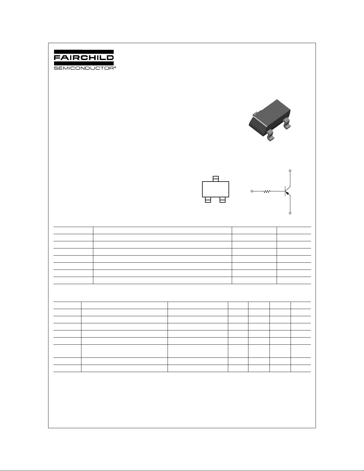
R81
3
1. Base 2. Emitter 3. Collector
Equivalent Circuit
R
B
PNP Epitaxial Silicon Transistor
Absolute Maximum Ratings
Symbol Parameter Value Units
V
V
V
I
P
T
T
CBO
CEO
EBO
C
C
J
STG
Collector-Base Voltage -40 V
Collector-Emitter Voltage -40 V
Emitter-Base Voltage -5 V
Collector Current -100 mA
Collector Power Dissipation 200 mW
Junction Temperature 150 °C
Storage Temperature -55 ~ 150 °C
Ta=25°C unless otherwise noted
1
2
SOT-23
C
E
Electrical Characteristics
Symbol Parameter Tes t Condition Min. Typ. Max. Units
BV
CBO
BV
CEO
I
CBO
h
FE
(sat) Collector-Emitter Saturation Voltage IC= -10mA, IB= -1mA -0.3 V
V
CE
C
ob
f
T
R Input Resistor 15 22 29 KΩ
©2002 Fairchild Semiconductor Corporation Rev. A, August 2002
Collector-Base Breakdown Voltage IC= -100µA, IE=0 -40 V
Collector-Emitter Breakdown Voltage IE= -1mA, IB=0 -40 V
Collector Cut-off Current VCB= -30V , IE=0 -0.1 µA
DC Current Gain VCE= -5V, IC= -1mA 100 600
Output Capacitance VCB= -10V , IE=0
Current Gain Bandwidth Product VCE= -10V , IC= -5mA 200 MHz
Ta=25°C unless otherwise noted
5.5 pF
f=1MHz
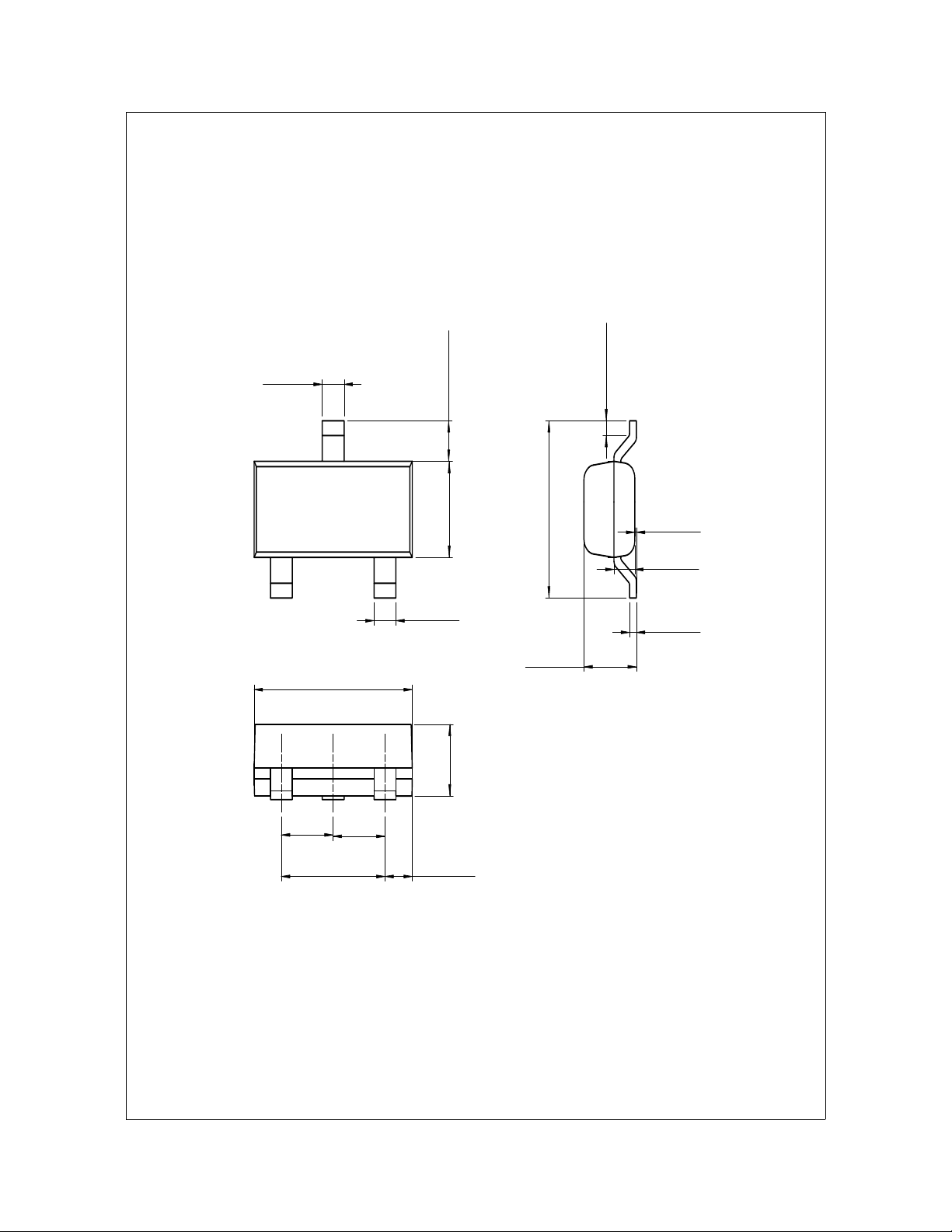
Package Dimensions
0.40
±0.03
FJV4111R
SOT-23
0.20 MIN
0.45~0.60
0.95
2.90
±0.03
1.90
±0.10
0.95
±0.03
±0.03
±0.10
0.40
±0.03
0.97REF 1.30
0.508REF
±0.10
2.40
0.96~1.14
0.03~0.10
0.38 REF
+0.05
0.12
–0.023
Dimensions in Millimeters
©2002 Fairchild Semiconductor Corporation Rev. A, August 2002
 Loading...