

Fairchild Semiconductor FJN3308R Datasheet
FJN3308R
Switching Application (Bias Resistor Built In)
• Switching circuit, Inverter, Interface circuit, Driver Circuit
• Built in bias Resistor (R
• Complement to FJN4308R
=47KΩ, R2=22KΩ)
1
FJN3308R
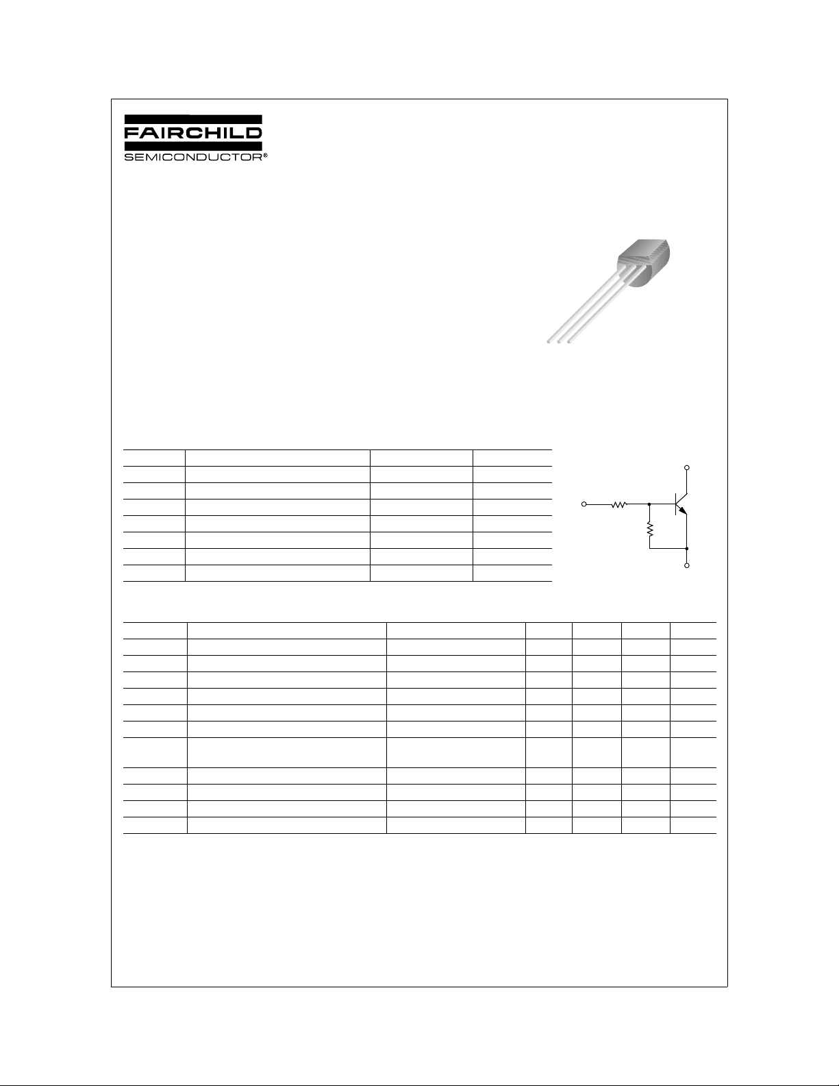
1
TO-92
1. Emitter 2. Collector 3. Base
NPN Epitaxial Silicon Transistor
Absolute Maximum Ratings
Symbol Parameter Value Units
V
V
V
I
P
T
T
CBO
CEO
EBO
C
C
J
STG
Collector-Base Voltage 50 V
Collector-Emitter Voltage 50 V
Emitter-Base Voltage 10 V
Collector Current 100 mA
Collector Power Dissipation 300 mW
Junction Temperature 150 °C
Storage Temperature -55 ~ 150 °C
Electrical Characteristics
Symbol Parameter Tes t Condition Min. Typ. Max. Units
BV
CBO
BV
CEO
I
CBO
h
FE
(sat) Collector-Emitter Saturation Voltage IC=10mA, IB=0.5mA 0.3 V
V
CE
f
T
C
ob
(off) Input Off Voltage VCE=5V, IC=100µA0.8 V
V
I
(on) Input On Voltage VCE=0.3V, IC=2mA 4 V
V
I
R
1
R
1/R2
Collector-Base Breakdown Voltage IC=10µA, IE=0 50 V
Collector-Emitter Breakdown Voltage IC=100µΑ, IB=0 50 V
Collector Cut-off Current VCB=40V, IE=0 0.1 µA
DC Current Gain VCE=5V, IC=5mA 56
Current Gain Bandwidth Product IC=10mA, IB=0.5mA 250 MHz
Output Capacitance VCB=10V, IE=0
Input Resistor 32 47 62 KΩ
Resistor Ratio 1.9 2.1 2.4
Ta=25°C unless otherwise noted
Ta=25°C unless otherwise noted
f=1.0MHz
Equivalent Circuit
R1
B
R2
3.7 pF
C
E
©2002 Fairchild Semiconductor Corporation Rev. A, August 2002
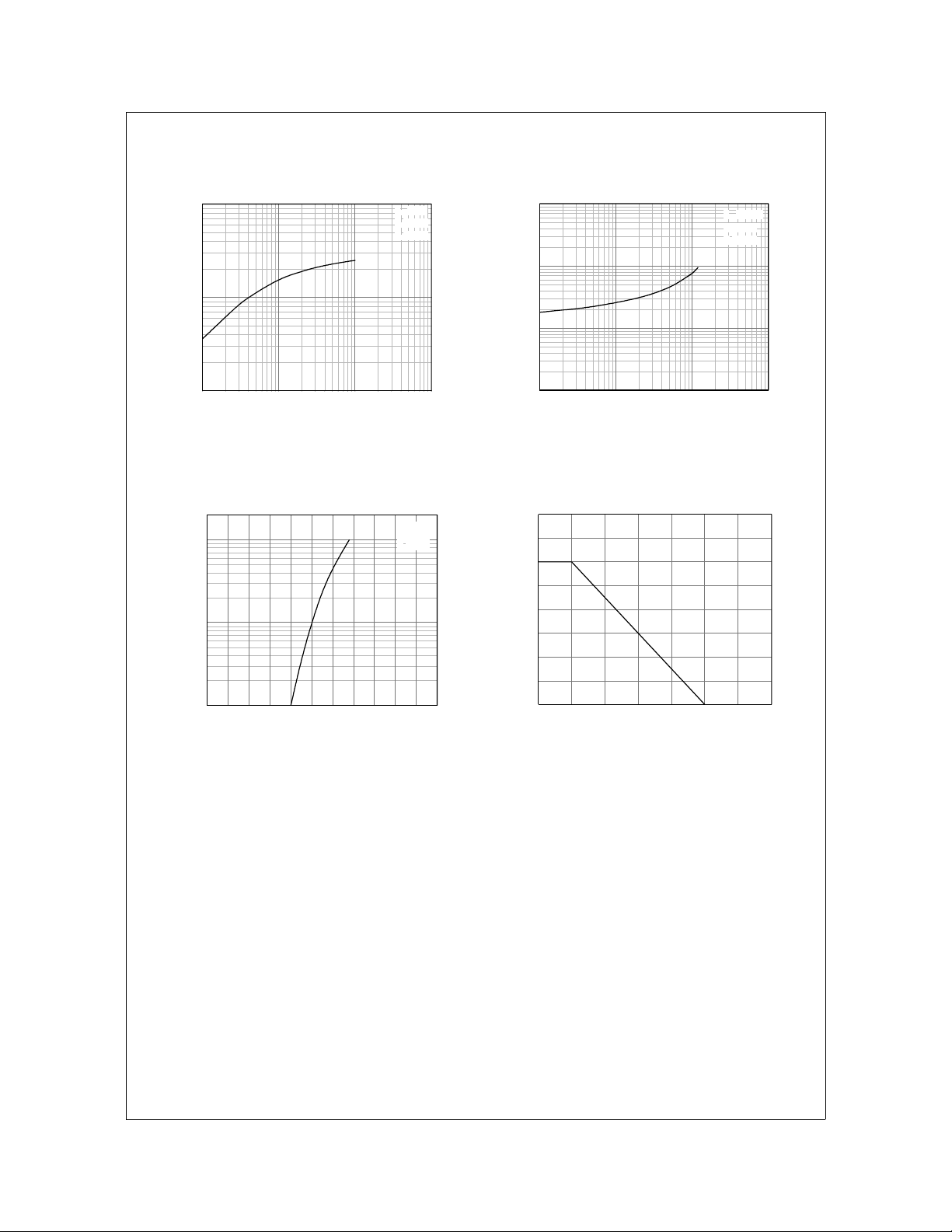
Typical Characteristics
FJN3308R
1000
100
, DC CURRENT GAIN
FE
h
10
1 10 100 1000
IC[mA], COLLECTOR CURRENT
Figure 1. DC current Gain Figure 2. Input On Voltage
1000
100
A], COLLECTOR CURRENT
µ
[
C
I
10
0.6 0.8 1.0 1.2 1.4 1.6 1.8 2.0 2.2 2.4 2.6 2.8
VI(off)[V], INPUT OFF VOLT AG E
VCE = 5V
R1 = 47K
R2 = 22K
VCE = 5V
R1 = 47K
R2 = 22K
100
VCE = 0.3V
R1 = 47K
R2 = 22K
10
1
(on)[V], INPUT VOLTAGE
I
V
0.1
0.1 1 10 100
IC[mA], COLLECTOR CURRENT
400
350
300
250
200
150
100
[mW], POWER DISSIPATION
C
P
50
0
0 25 50 75 100 125 150 175
Ta[oC], AMBIENT TEMPERATURE
Figure 3. Input Off Voltage Figure 4. Power Derating
©2002 Fairchild Semiconductor Corporation
Rev. A, August 2002
 Loading...