

Fairchild Semiconductor FFB3946 Datasheet

FFB3946 / FMB3946
FFB3946
C1
SC70-6
Mark: .AB
Dot denotes pin #1
B2
E2
pin #1
TRANSISTOR TYPE
C1 B1 E1 NPN
C2
B1
E1
C2 B2 E2 PNP
FMB3946
E1
C1
SuperSOT-6
Mark: .002
Dot denotes pin #1
C2
pin #1
B1
B2
E2
NPN & PNP General Purpose Amplifier
This complementary device is designed for use as a general purpose
amplifier and switch The useful dynamic range extends to 100 mA as a
switch and 100 MHz as an amplifier. Sourced from Process 23 and 66.
See FFB3904 (NPN) and FFB3906 (PNP) for characteristics.
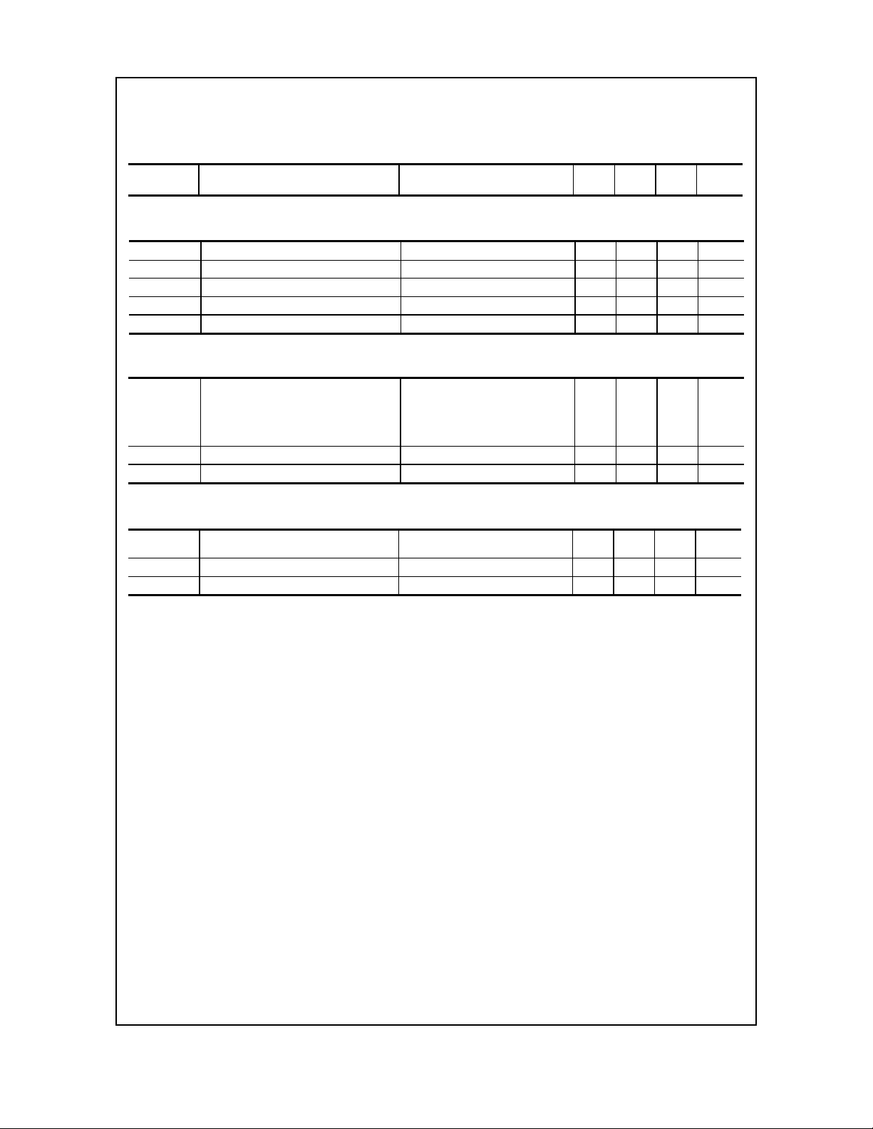
Absolute Maximum Ratings* T
Symbol Parameter Value Units
V
CEO
V
CBO
V
EBO
I
C
TJ, T
stg
*These ratings are limiting values above which the serviceability of any semiconductor device may be impaired.
NOTES:
1) These ratings are based on a maximum junction temperature of 150 degrees C.
2) These are steady state limits. The factory should be consulted on applications involving pulsed or low duty cycle operations.
3) All voltages (V) and currents (A) are negative polarity for PNP transistors.
Collector-Emitter V ol tage 40 V
Collector-Base Voltage 40 V
Emitter-Base Volt age 5.0 V
Collector Current - Continuous 200 mA
Operating and Storage Junction Temperature Range -55 to +150
= 25°C unless otherwise noted
A
C
°
4
Thermal Characteristics T
= 25°C unless otherwise noted
A
Symbol Characteristic Max Units
FFB3946 FMB3946
P
D
R
JA
θ
1999 Fairchild Semiconductor Corporation
Total Device Dissipation
Derate above 25°C
300
2.4
700
5.6
Thermal Resistance, Junction to Ambient 415 180
mW
mW/°C
C/W
°
NPN & PNP General Purpose Amplifier
(continued)
FFB3946 / FMB3946
Electrical Characteristics T
= 25°C unless otherwise noted
A
Symbol Parameter Test Conditions Min Typ Max Units
OFF CHARACTERISTICS
V
(BR)CEO
V
(BR)CBO
V
(BR)EBO
I
CBO
I
EBO
Collector-Emitter B reakdown Voltage IC = 10 mA, IB = 0 40 V
Collector-Base Breakdown Voltage
Emitter-Base Breakdown Volt age
I
= 10 µA, IE = 0
C
I
= 10 µA, IC = 0
E
Collector Cutoff Current VCB = 30 V, I
Emitter Cutoff Current VEB = 4.0 V, I
= 0 50 nA
E
= 0 50 nA
C
40 V
5.0 V
ON CHARACTERISTICS
h
FE
V
sat
CE(
V
sat
BE(
DC Current Gain
Collector-Emitter Saturation Voltage IC = 10 mA, IB = 1.0 mA 0.25 V
)
Base-Emitter Saturation Voltage IC = 10 mA, IB = 1.0 mA 0.9 V
)
I
= 100 µA, VCE = 1.0 V
C
= 1.0 mA, VCE = 1.0 V
I
C
= 10 mA, VCE = 1.0 V
I
C
= 50 mA, VCE = 1.0 V
I
C
= 100mA, VCE = 1.0 V
I
C
40
70
100
60
30
300
SMALL SIGNAL CHARACTERISTICS
f
T
C
obo
C
ibo
Current Gain - Bandwidth Product IC = 10 mA, VCE = 20 V,
200 MHz
f = 100 MHz
Output Capacitance VCB = 5.0 V, f = 100 kHz 4.5 pF
Input Capacitance VCB = 5.0 V, f = 100 kHz 10 pF
NOTE: All voltages (V) and currents (A) are negative polarity for PNP transistors.
 Loading...