

Fairchild Semiconductor FFA20U120DN Datasheet
FFA20U120DN
Features
• High v ol tage and high rel ia bi lity
• High speed switching
• Low forward voltage
Applications
• General purpose
• Switc hing mode power supply
• Free-wheeling diode for motor application
• Power switching circuits
1 2 3
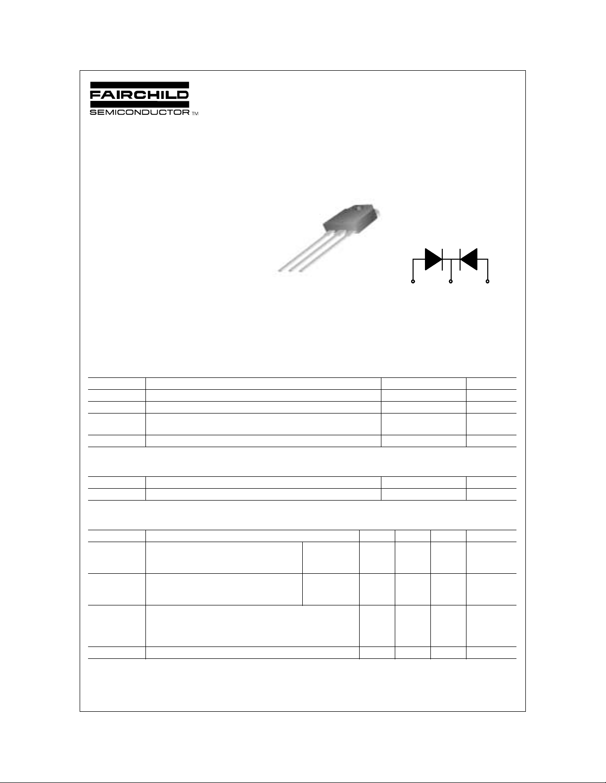
ULTRA FAST RECOVERY POWER RECTIFIER
TO-3P
FFA20U120DN
1. Anode 2.Cathode 3. Anode
Absolute Maximum Ratings
Symbol Parameter Value Units
V
RRM
I
F(AV)
I
FSM
T
J, TSTG
Peak Repetitiv e Reverse Volt age 1200 V
Average Rectified Forward Current @ TC = 100°C20 A
Non-repetitive Peak Surge Current
60Hz Single Ha lf- Sine Wave
Operating Junction and Storage Temperature - 65 to +150 °C
(per diode) TC=25°°°°C unless otherwise noted
120 A
Thermal Characteristics
Symbol Parameter Value Units
R
θJC
Electrical C haract eri stics
Symbol Parameter Min. Typ. Max. Units
V
FM
*
I
RM
*
t
rr
I
rr
Q
rr
W
AVL
* Pulse Test: Pulse Width=300µs, Duty Cycle=2%
Maxi mum Therm al Resistance, Junction to Case 0.84 °C/W
(per diode) TC=25 °°°°C unless otherwise noted
Maximum Instantaneous Forward Voltage
I
I
Maximum Instantaneous Reverse Current
Maximum Reverse Recovery Time
Maximum Reverse Recovery Current
Maximum Reverse Recovery Charge
(I
=20A, di/dt = 200A/µs)
F
Avalanche Energy 1.0 - - mJ
= 20A
F
= 20A
F
@ rated V
= 25 °C
T
C
T
= 100 °C
C
TC = 25 °C
R
T
= 100 °C
C
-
-
-
-
-
-
-
-
-
-
-
-
-
-
3.5
3.2
20
1.2
120
10
500
V
µA
mA
ns
A
nC
©2000 Fai r ch i ld Semiconductor Inter national
Rev. F, September 2000
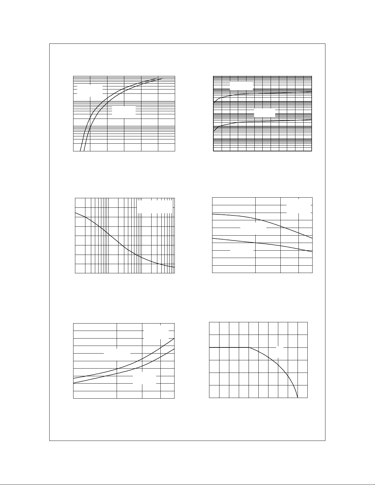
Typical C h aracteristic s
FFA20U120DN
100
TC = 100oC
[A]
F
10
TC = 25oC
1
Forward Current , I
0.1
0123456
Forward Voltage , VF [V]
Figure 1. Typical Forward Voltage Drop
vs. Forward Current
400
350
300
250
200
150
100
Capacit anc e , Cj [ pF]
50
0.1 1 10 100
Reverse Voltage , VR [V]
Typical Capacitan ce
at 0V = 355 pF
1000
100
A]
µ
[
R
10
1
0.1
Reverse Current , I
0.01
0.001
0 200 400 600 800 1000 1200
TC = 100oC
TC = 25oC
Reverse Voltage , VR [V]
Figure 2. Typical Reverse Current
vs. Revers e Voltag e
140
VR = 200V
120
[ns]
rr
100
80
60
Reverse Recovery Time , t
40
100 500
TC = 100oC
TC = 25oC
di/dt [A/µs]
IF = 20A
Figure 3. Typical Junction Capacitance
Figure 4. Typical Reverse Recovery Time
vs. di/dt
25
VR = 200V
[A]
rr
20
15
10
5
Reverse Recovery Current , I
0
100 500
TC = 100oC
IF = 20A
TC = 25oC
di/dt [A/µs]
Figure 5. Typical Reverse Recovery Current
30
[A]
25
F(AV)
20
15
10
5
DC
Averag e Forwa rd Cur rent , I
0
60 80 100 120 140 160
Case Temperature , TC [oC]
Figure 6. Forward Current Derati ng Curve
vs. di/dt
©2000 Fai r ch i ld Semiconductor Inter national Rev. F, September 2000
 Loading...