

Fairchild Semiconductor FDS6676 Datasheet
May 2003
G
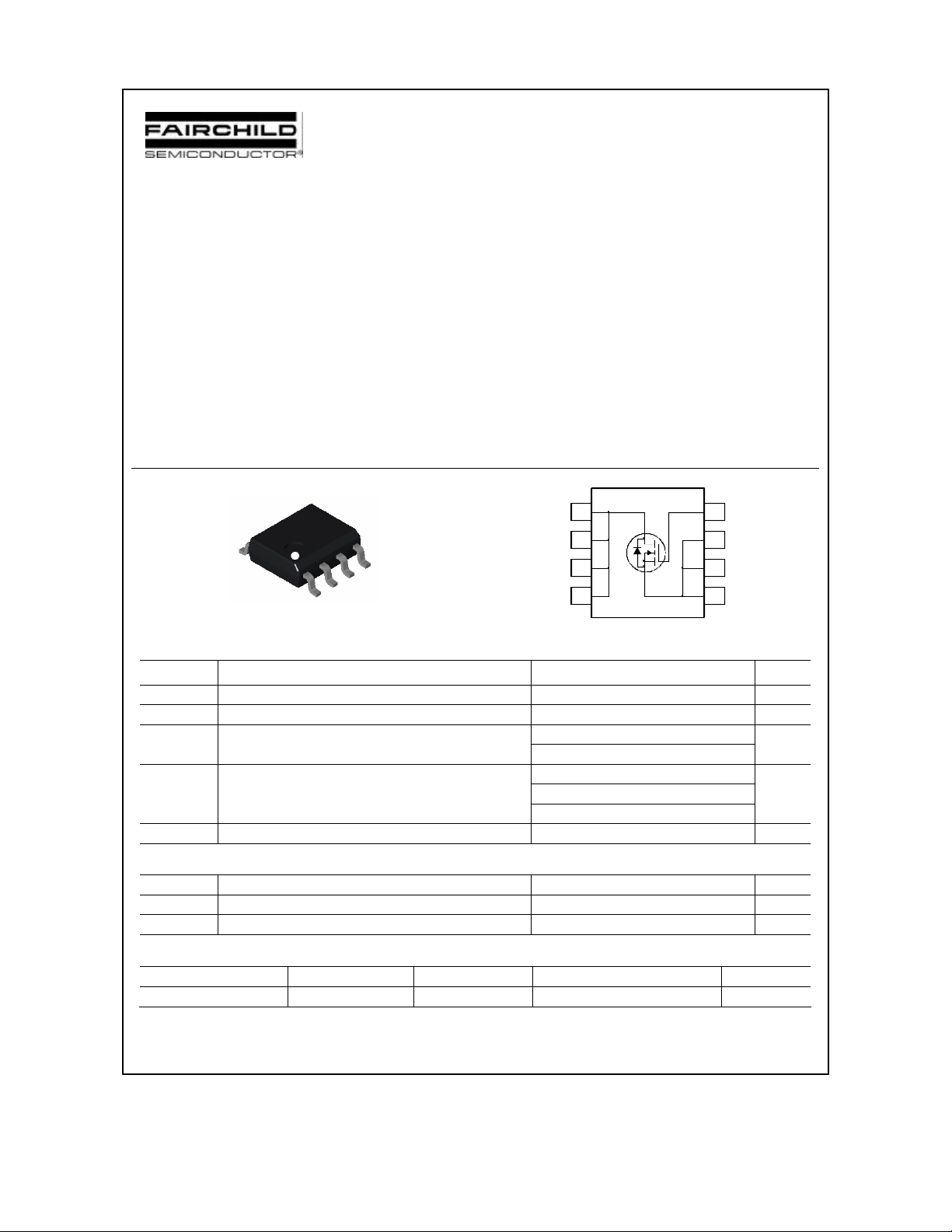
FDS6676
FDS6676
30V N-Channel PowerTrench MOSFET
General Description
This N-Channel MOSFET has been designed
specifically to improve the overall efficiency of DC/DC
converters using either synchronous or conventional
switching PWM controllers. It has been optimized for
low gate charge, low R
and fast switching speed.
DS(ON)
Applications
• DC/DC converter
D
D
D
D
S
SO-8
Absolute Maximum Ratings T
S
S
o
=25
C unless otherwise noted
A
Features
• 14.5 A, 30 V. R
R
• High performance trench technology for extremely
low R
• Low gate charge (45 nC typ)
• High power and current handling capability
DS(ON)
5
6
7
8
= 7 mΩ @ VGS = 10 V
DS(ON)
= 8 mΩ @ VGS = 4.5 V
DS(ON)
4
3
2
1
Symbol Parameter Ratings Units
V
Drain-Source Voltage 30 V
DSS
V
Gate-Source Voltage
GSS
ID Drain Current – Continuous (Note 1a) 14.5 A
– Pulsed 50
PD
TJ, T
STG
Power Dissipation for Single Operation (Note 1a) 2.5
(Note 1b)
(Note 1c)
Operating and Storage Junction Temperature Range –55 to +175
± 16
1.2
1.0
°C
V
W
Thermal Characteristics
R
θJA
R
θJA
R
θJC
Thermal Resistance, Junction-to-Ambient (Note 1a) 50
Thermal Resistance, Junction-to-Ambient (Note 1c) 125
Thermal Resistance, Junction-to-Case (Note 1) 25
Package Marking and Ordering Information
Device Marking Device Reel Size Tape width Quantity
2003 Fairchild Semiconductor Corporation
FDS6676 FDS6676 13’’ 12mm 2500 units
°C/W
°C/W
°C/W
FDS6676 Rev D (W)
FDS6676
Electrical Characteristics T
Symbol
Parameter Test Conditions Min Typ Max Units
= 25°C unless otherwise noted
A
Drain-Source Avalanche Ratings (Note 2)
W
Single Pulse Drain-Source
DSS
Avalanche Energy
IAR Maximum Drain-Source
VDD = 15 V, ID = 20 A
370
mJ
20 A
Avalanche Current
Off Characteristics
BV
Drain–Source Breakdown Voltage
DSS
∆BVDSS
∆TJ
I
Zero Gate Voltage Drain Current VDS = 24 V, VGS = 0 V 1
DSS
I
GSSF
I
GSSR
Breakdown Voltage Temperature
Coefficient
Gate–Body Leakage, Forward VGS = 16 V, VDS = 0 V 100 nA
Gate–Body Leakage, Reverse VGS = –16 V, VDS = 0 V –100 nA
VGS = 0 V, ID = 250 µA
ID = 250 µA, Referenced to 25°C
30 V
24
mV/°C
µA
On Characteristics (Note 2)
V
Gate Threshold Voltage
GS(th)
∆VGS(th)
∆TJ
R
DS(on)
Gate Threshold Voltage
Temperature Coefficient
Static Drain–Source
On–Resistance
I
On–State Drain Current VGS = 10 V, VDS = 5 V 50 A
D(on)
gFS Forward Transconductance VDS = 5 V, ID = 14.5 A 80 S
VDS = VGS, ID = 250 µA
ID = 250 µA, Referenced to 25°C
VGS = 10 V, ID = 14.5 A
VGS = 4.5 V, ID = 13.5 A
VGS = 10 V, ID = 14.5 A, TJ = 125°C
1 1.5 3 V
7
8
11.5
mV/°C
mΩ
–5
4.8
5.4
7.3
Dynamic Characteristics
C
Input Capacitance 5103 pF
iss
C
Output Capacitance 836 pF
oss
C
Reverse Transfer Capacitance
rss
VDS = 15 V, V
f = 1.0 MHz
= 0 V,
GS
361 pF
Switching Characteristics (Note 2)
t
Turn–On Delay Time 15 27 ns
d(on)
tr Turn–On Rise Time 9 18 ns
t
Turn–Off Delay Time 87 139 ns
d(off)
tf Turn–Off Fall Time
Qg Total Gate Charge 45 63 nC
Qgs Gate–Source Charge 13 nC
Qgd Gate–Drain Charge
VDD = 15 V, ID = 1 A,
VGS = 10 V, R
GEN
= 6 Ω
VDS = 15 V, ID = 14.5 A,
VGS = 5 V
40 64 ns
12 nC
Drain–Source Diode Characteristics and Maximum Ratings
IS Maximum Continuous Drain–Source Diode Forward Current 2.1 A
VSD
Drain–Source Diode Forward
Voltage
VGS = 0 V, IS = 2.1 A (Note 2) 0.7 1.2 V
FDS6676 Rev D (W)
 Loading...