

Fairchild Semiconductor FDFS6N303 Datasheet
October 2001
FDFS6N303
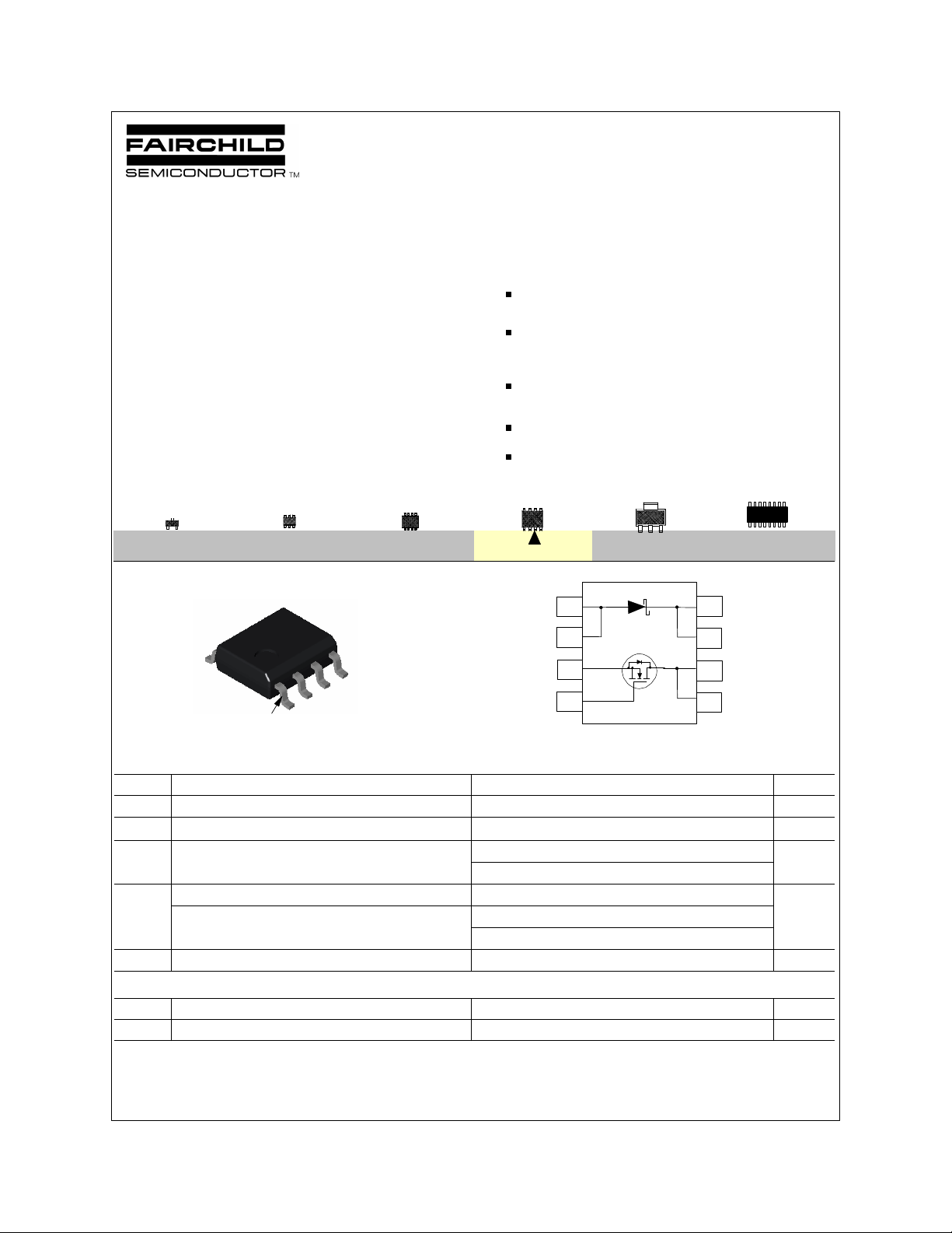
N-Channel MOSFET with Schottky Diode
General Description Features
Fairchild Semiconductor's FETKEY technology incorporates
a high cell density MOSFET and low forward drop (0.35V)
Schottky diode into a single surface mount power package.
The MOSFET and Schottky diode are isolated inside the
package. The general purpose pinout has been chosen to
maximize flexibility and ease of use. FETKEY products are
particularly suited for switching applications such as DC/DC
buck, boost, synchronous, and non-synchronous converters
where the MOSFET is driven as low as 4.5V and fast
switching, high efficiency and small PCB footprint is
desirable.
SOT-23
TM
-6
D
D
SuperSOT
TM
-8
C
C
FDFS
6N303
G
S
SO-8
pin
A
1
A
6 A, 30 V. R
R
= 0.035 Ω @ VGS = 10 V.
DS(ON)
= 0.050 Ω @ VGS = 4.5 V.
DS(ON)
VF < 0.28 V @ 0.1 A
< 0.42 V @ 3 A
V
F
< 0.50 V @ 6 A.
V
F
Schottky and MOSFET incorporated into single power
surface mount SO-8 package.
General purpose pinout for design flexibility.
Ideal for DC/DC converter applications.
SO-8 SOT-223SuperSOT
A
1
A C
2
S
3
G
4
SOIC-16
C
8
7
D
6
D
5
MOSFET Maximum Ratings T
= 25oC unless otherwise noted
A
Symbol Parameter FDFS6N303 Units
V
DSS
V
GSS
I
D
Drain-Source Voltage 30 V
Gate-Source Voltage ±20 V
Drain Current - Continuous (Note 1a) 6 A
- Pulsed 30
P
D
T
J,TSTG
Schottky Diode Maximum Ratings T
V
RRM
I
O
© 2001 Fairchild Semiconductor Corporation FDFS6N303 Rev. D1
Power Dissipation for Dual Operation 2 W
Power Dissipation for Single Operation
(Note 1c) 0.9
(Note 1a) 1.6
Operating and Storage Temperature Range -55 to 150 °C
= 25oC unless otherwise noted
A
Repetitive Peak Reverse Voltage 30 V
Average Forward Current (Note 1a) 2 A
Electrical Characteristics (T
= 25 oC unless otherwise noted )
A
MOSFET ELECTRICAL CHARACTERISTICS
Symbol Parameter Conditions Min Typ Max Units
BV
DSS
I
DSS
I
GSSF
I
GSSR
V
GS(th)
R
DS(ON)
Drain-Source Breakdown Voltage VGS = 0 V, I D = 250 µA 30 V
Zero Gate Voltage Drain Current VDS = 24 V, V
= 0 V 1 µA
GS
=125°C 20 µA
T
J
Gate - Body Leakage, Forward VGS = 20 V, VDS = 0 V 100 nA
Gate - Body Leakage, Reverse VGS = -20 V, VDS= 0 V -100 nA
Gate Threshold Voltage VDS = VGS, ID = 250 µA 1 1.7 3 V
Static Drain-Source On-Resistance VGS = 10 V, I D = 6 A 0.025 0.035
Ω
VGS = 4.5 V, I D = 4.8 A 0.043 0.05
g
I
D(ON)
C
C
C
Q
t
D(on)
t
r
t
D(off)
t
f
FS
iss
oss
rss
g
Forward Transconductance VDS = 10 V, ID = 6 A 12 S
On-State Drain Current VGS = 10 V, VDS = 5 V 15 A
Input Capacitance VDS = 15 V, VGS = 0 V, 350 pF
Output Capacitance f = 1.0 MHz 220 pF
Reverse Transfer Capacitance 80 pF
Total Gate Charge VDS = 15 V, ID = 6 A, VGS = 10 V 12 17 nC
Turn - On Delay Time VDD = 10 V, ID = 1 A,
V
= 4.5 V, R
Turn - On Rise Time 12 25 ns
GS
GEN
= 6 Ω
7.5 15 ns
Turn - Off Delay Time 13 25 ns
Turn - Off Fall Time 6 15 ns
MOSFET DRAIN-SOURCE DIODE CHARACTERISTICS AND MAXIMUM RATINGS
I
S
V
SD
Maximum Continuous Drain-Source Diode Forward Current 1.3 A
Drain-Source Diode Forward Voltage VGS = 0 V, I S = 1.3 A (Note 2) 0.8 1.2 V
SCHOTTKY DIODE CHARACTERISTICS
B
V
I
R
V
F
Reverse Breakdown Voltage IR = 1 mA 30 V
Reverse Leakage VR = 30 V 0.5 mA
Forward Voltage IF = 0.1 A 280 mV
= 3 A 420
I
F
= 6 A 500
I
F
THERMAL CHARACTERISTICS
R
JA
θ
R
JC
θ
Notes:
1. R
JA
θ
guaranteed by design while R
Thermal Resistance, Junction-to-Ambient (Note 1a) 78 °C/W
Thermal Resistance, Junction-to-Case (Note 1) 40 °C/W
is the sum of the junction-to-case and case-to-ambient thermal resistance where the case thermal reference is defined as the solder mounting surface of the drain pins. R
is determined by the user's board design.
CA
θ
JC
θ
is
Scale 1 : 1 on letter size paper
2. Pulse Test: Pulse Width <
300µs, Duty Cycle < 2.0%.
a. 78OC/W on a 0.5 in
pad of 2oz copper.
2
b. 125OC/W on a 0.02 in
pad of 2oz copper.
2
c. 135OC/W on a 0.003 in
pad of 2oz copper.
FDFS6N303 Rev. D1
2
 Loading...