

Fairchild Semiconductor FDFS2P106A Datasheet
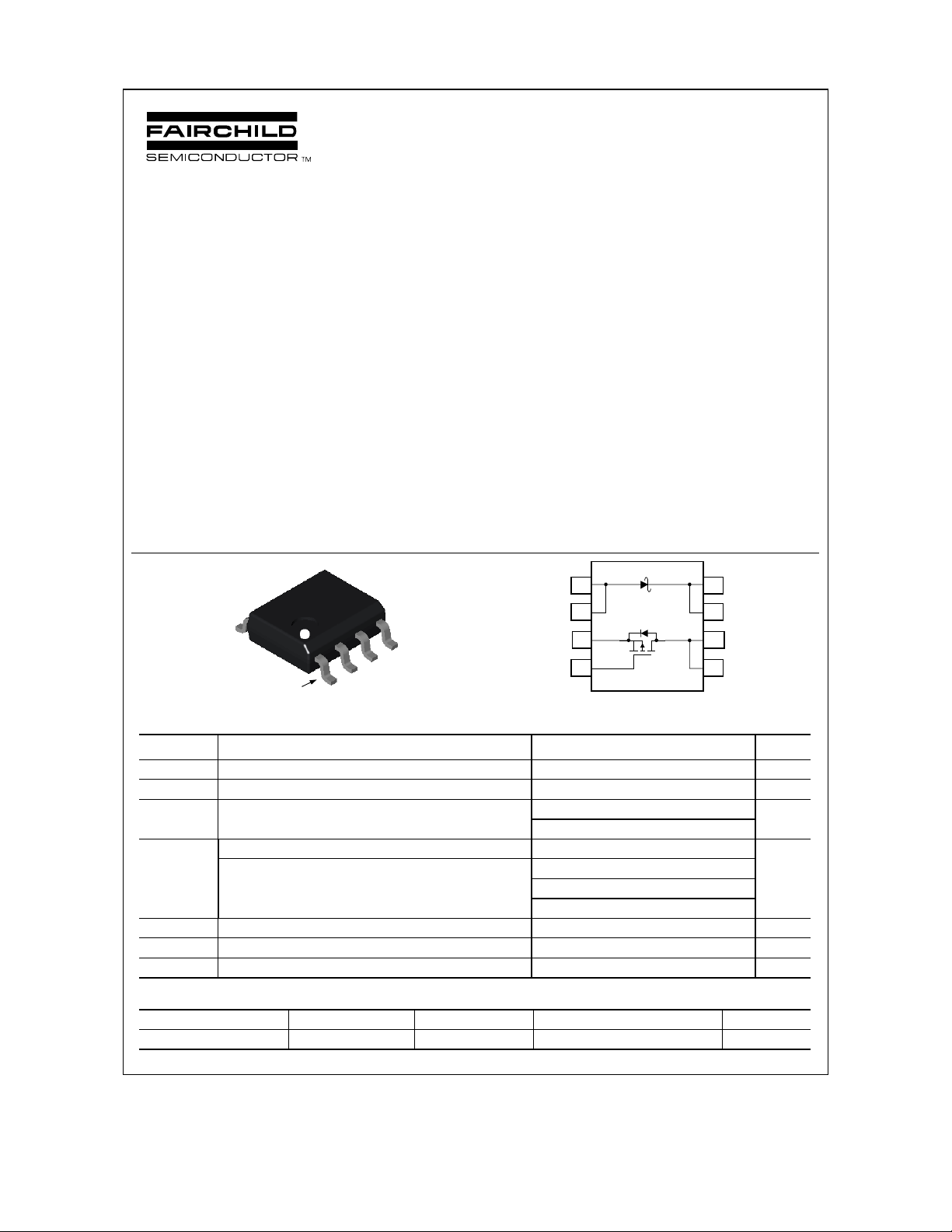
FDFS2P106A
Integrated 60V P-Channel PowerTrench
June 2001
MOSFET and Schottky Diode
FDFS2P106A
General Description
The FDFS2P106A combines the exceptional
performance of Fairchild's PowerTrench MOSFET
technology with a very low forward voltage drop
Schottky barrier recti fier in an SO-8 package.
This device is designed specifically as a single package
solution for DC to DC converters. It features a fast
switching, low gate charge MOSFET with very low onstate resistance. The independently connected
Schottky diode allows its use in a variety of DC/DC
converter topologies.
D
D
C
C
SO-8
Pin 1
A
Absolute Maximum Ratings T
G
S
A
o
=25
C unless otherwise noted
A
Features
• –3.0 A, –60V R
R
• V
< 0.45 V @ 1 A (TJ = 125°C)
F
V
< 0.53 V @ 1 A
F
V
< 0.62 V @ 2 A
F
• Schottky and MOSFET incorporated into single
power surface mount SO-8 package
• Electrically independent S chottky and MOSFET
pinout for design flexibility
A
A
S
G
= 110 mΩ @ VGS = –10 V
DS(ON)
= 140 mΩ @ VGS = –4.5 V
DS(ON)
81
72
63
54
C
C
D
D
Symbol Parameter Ratings Units
V
MOSFET Drain-Source Voltage
DSS
V
MOSFET Gate-Source Voltage
GSS
ID Drain Current – Continuous (Note 1a)
– Pulsed
PD
TJ, T
STG
V
Schottky Repetiti ve P eak Reverse Voltage 45 V
RRM
IO Schottky Average Forward Current (Note 1a) 1 A
Power Dissipation for Dual Operation 2
Power Dissipation for Single Operation (Note 1a) 1.6
(Note 1b)
Operating and Storage Junction Temperature Range
(Note 1c)
–60
±20
–3
–10
1
0.9
–55 to +150
V
V
A
W
°C
Package Marking and Ordering Information
Device Marking Device Reel Size Tape width Quantity
FDFS2P106A FDFS2P106A 13’’ 12mm 2500 units
2001 Fairchild Semiconductor Corporation
FDFS2P106A Rev B(W)
FDFS2P106A
Electrical Characteristics T
= 25°C unless otherwise noted
A
Symbol Parameter Test Conditions Min Typ Max Units
Off Characteristics
BV
Drain–Source Breakdown Voltage
DSS
∆BVDSS
∆T
I
Zero Gate Voltage Drain Current VDS = –48 V, VGS = 0 V –1
DSS
I
GSSF
I
GSSR
Breakdown Voltage Temperature
Coefficient
J
Gate–Body Leakage, Forward VGS = 20V, VDS = 0 V 100 nA
Gate–Body Leakage, Reverse VGS = –20 V VDS = 0 V –100 nA
= 0 V, ID = –250 µA
V
GS
= –250 µA, Referenced to 25°C
I
D
–60 V
–60
mV/°C
µA
On Characteristics (Note 2)
V
Gate Threshold Voltage
GS(th)
∆VGS(th)
∆TJ
R
DS(on)
Gate Threshold Voltage
Temperature Coefficient
Static Drain–Source
On–Resistance
I
On–S t ate Drain Current VGS = –10 V, VDS = –5 V –10 A
D(on)
= VGS, ID = –250 µA
V
DS
= –250 µA,Referenced to 25°C
I
D
VGS = –10 V, ID = –3A
= –4.5 V, ID = –2.7 A
V
GS
= –10 V, ID = –3 A, TJ=125°C
V
GS
gFS Forward Transconductance VDS = –5 V, ID = –3.3 A 8 S
–1 –1.6 –3 V
4
91
112
150
110
140
192
mV/°C
mΩ
Dynamic Characteristics
C
Input Capacitance 714 pF
iss
C
Output Capacitance 84 pF
oss
C
Reverse Transfer Capacitance
rss
= –30 V, V
V
DS
f = 1.0 MHz
= 0 V,
GS
33 pF
Switching Characteristics (Note 2)
t
Turn–On Delay Time 8 15 ns
d(on)
tr Turn–On Rise Time 11 19 ns
t
Turn–Off Delay Time 28 45 ns
d(off)
tf Turn–Off Fall Time
Qg Total Gate Charge 15 21 nC
Qgs Gate–Source Charge 2 nC
Qgd Gate–Drain Charge
= –30 V, ID = –1 A,
V
DD
= –10 V, R
V
GS
= –30V, ID = –3A,
V
DS
V
= –10 V
GS
GEN
= 6 Ω
8.5 17 ns
3 nC
Drain–Source Diode Characteristics and Maximum Ratings
IS Maximum Continuous Drain–Source Diode Forward Current –1.3 A
VSD Drain–Source Diode Forward
Voltage
VGS = 0 V, IS = –1.3 A (Note 2) –0.8 –1.2 V
FDFS2P106A Rev B(W)
 Loading...