

Fairchild Semiconductor FDU7030BL, FDD7030BL Datasheet
FDD7030BL/FDU7030BL
FDD7030BL/FDU7030BL
30V N-Channel PowerTrench MOSFET
June 2003
General Description
This N-Channel MOSFET has been designed
specifically to improve the overall efficiency of DC/DC
converters using either synchronous or conventional
switching PWM controllers. It has been optimized for
low gate charge, low RDS( ON) , fast switching speed and
extremely low R
in a small package.
DS(ON)
Features
• 56 A, 30 V R
R
• Low gate charge
• Fast Switching
= 9.5 mΩ @ VGS = 10 V
DS(ON)
= 13 mΩ @ VGS = 4.5 V
DS(ON)
Applications
• DC/DC converter
• Motor Drives
• High performance trench technology for extremely
low R
DS(ON)
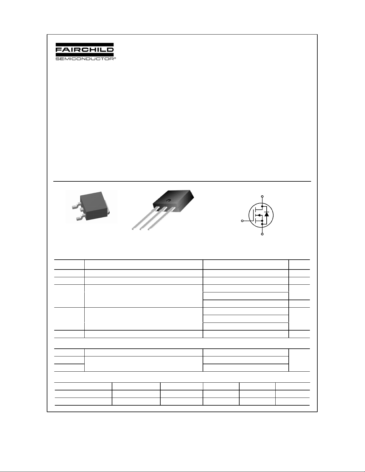
D
D
G
S
D-PAK
TO-252
(TO-252)
G D S
Absolute Maximum Ratings T
I-PAK
(TO-251AA)
=25oC unless otherwise noted
A
G
S
Symbol Parameter Ratings Units
V
DSS
V
GSS
I
D
P
D
TJ, T
STG
Drain-Source Voltage 30 V
Gate-Source Voltage
Continuous Drain Current @TC=25°C (Note 3) 56 A
@TA=25°C (Note 1a) 14
Pulsed (Note 1a) 100
Power Dissipation @TC=25°C (Note 3) 60
@TA=25°C (Note 1a) 2.8
@TA=25°C (Note 1b) 1.3
Operating and Storage Junction Temperature Range –55 to +175
±20
V
W
°C
Thermal Characteristics
R
θJC
R
θJA
R
θJA
Thermal Resistance, Junction-to-Case (Note 1) 2.5
Thermal Resistance, Junction-to-Ambient (Note 1a) 45
Package Marking and Ordering Information
Device Marking Device Package Reel Size Tape width Quantity
FDD7030BL FDD7030BL D-PAK (TO-252) 13’’ 12mm 2500 units
FDU7030BL FDU7030BL I-PAK (TO-251) Tube N/A 75
2003 Fairchild Semiconductor Corp.
(Note 1b)
°C/W
96
FDD7030BL/FDU7030BL Rev CW)
Electrical Characteristics T
FDD7030BL/FDU7030BL
= 25°C unless otherwise noted
A
Symbol Parameter Test Conditions Min Typ Max Units
Drain-Source Avalanche Ratings (Note 2)
E
AS
I
AS
Drain-Source Avalanche Energy Single Pulse, VDD = 15 V, ID= 14A 174 mJ
Drain-Source Avalanche Current 14 A
Off Characteristics
BV
DSS
∆BVDSS
∆T
I
DSS
I
GSS
Drain–Source Breakdown Voltage
Breakdown Voltage Temperature
Coefficient
J
VGS = 0 V, ID = 250 µA
ID = 250 µA,Referenced to 25°C
Zero Gate Voltage Drain Current VDS = 24 V, VGS = 0 V 1
Gate–Body Leakage
VGS = ±20 V, VDS = 0 V ±100
30 V
26
mV/°C
µA
nA
On Characteristics (Note 2)
V
GS(th)
∆VGS(th)
∆T
R
DS(on)
I
D(on)
g
FS
Gate Threshold Voltage
Gate Threshold Voltage
Temperature Coefficient
J
Static Drain–Source
On–Resistance
VDS = VGS, ID = 250 µA
ID = 250 µA,Referenced to 25°C
VGS = 10 V, ID = 14 A
VGS = 4.5 V, ID = 12 A
VGS = 10 V, ID = 14 A,TJ=125°C
1 1.8 3 V
–5
7.5
9.6
11
On–State Drain Current VGS = 10 V, VDS = 5 V 50 A
Forward Transconductance VDS = 10 V, ID = 14 A 56 S
9.5
13
16
mV/°C
mΩ
Dynamic Characteristics
C
iss
C
oss
C
rss
R
G
Input Capacitance 1425 pF
Output Capacitance 350 pF
Reverse Transfer Capacitance
Gate Resistance V
VDS = 15 V, V
f = 1.0 MHz
= 15 mV, f = 1.0 MHz 1.3 pF
OSC
GS
= 0 V,
150 pF
Switching Characteristics (Note 2)
t
t
t
t
Q
Q
Q
d(on)
r
d(off)
f
g
gs
gd
Turn–On Delay Time 11 20 ns
Turn–On Rise Time 9 18 ns
Turn–Off Delay Time 31 50 ns
Turn–Off Fall Time
VDD = 15 V, ID = 1 A,
VGS = 10 V, R
GEN
= 6 Ω
13 23 ns
Total Gate Charge 14 20 nC
Gate–Source Charge 4 nC
Gate–Drain Charge
VDS = 15V, ID = 14 A,
VGS = 5 V
5 nC
FDD7030BL/FDU7030BL Rev. B(W)
 Loading...