

Fairchild Semiconductor FDD6680A Datasheet
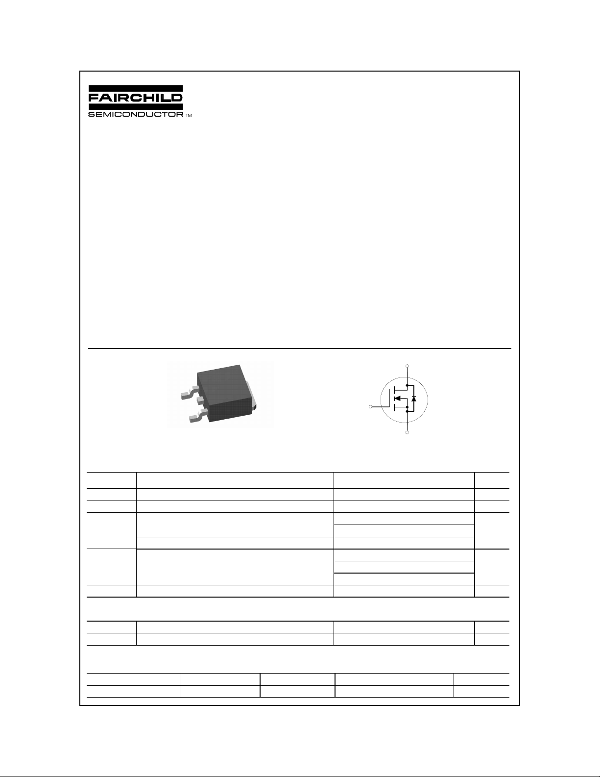
FDD6680A
N-Channel, Logic Level, PowerTrench
MOSFET
FDD6680A
February 2000
General Description
This N-Channel Logic level MOSFET is produced using
Fairchild Semiconductor's advanced PowerTrench process
that has been especially tailored to minimize the on-state
resistance and yet maintain low gate charge for superior
switching performance.
Features
• 56 A, 30 V. R
R
DS(ON)
DS(ON)
= 0.0095 Ω @ V
= 0.0130 Ω @ V
• Low gate charge ( 23nC typical ).
= 10 V
GS
= 4.5 V.
GS
• Fast switching speed.
Applications
• DC/DC converter
• High performance trench technology for extremely
low R
DS(ON)
.
• Motor drives
D
D
G
G
S
±20
56
14
2.8
S
V
A
W
°C
TO-252
Absolute Maximum Ratings
Symbol Parameter Ratings Units
V
DSS
V
GSS
I
D
P
D
TJ, T
stg
Drain-Source Voltage 30 V
Gat e-Source Voltage
Maximum Drain Current - Continuous
(Note 1a)
Maximum Drain Current - Pulsed 100
Maximum Power Dissipation @ TC = 25oC (Note 1) 60
TA = 25oC (Note 1b) 1.3
Operatin g and Storage Junction Temperature Rang e -55 to +150
=25oC unless otherwise noted
T
A
(Note 1)
TA = 25oC
(Note 1a)
Thermal Characteristics
R
θ
JC
R
θ
JA
Thermal Resistance, Junction-to-Case (Note 1) 2.1
Thermal Resistance, Junction-to-Ambient
(Note 1b)
96
Package Marking and Ordering Information
Device Marking Device Reel Size Tape width Quantity
FDD6680A FDD6680A 13’’ 16mm 2500
2000 Fairchild Semiconductor Corporation
°C/W
°C/W
FDD6680A, Rev. C
Electrical Characteri stics T
= 25°C unless otherwise not ed
A
Symbol Parameter Test Conditions Min Typ Max Units
FDD6680A
Drain-Source Avalanche Ratings
W
DSS
I
AR
Single Pul se Drain-Sour c e
Avalanche Energy
Maximum Drain-Source Avalanche Current 56 A
Off Characteristics
BV
DSS
DSS
∆
BV
∆
T
J
I
DSS
I
GSSF
I
GSSR
On Characteristics
V
GS(th)
GS(th)
∆
V
∆
T
J
R
DS(on)
I
D(on)
g
FS
Drain-Source Breakdown Voltage
Breakdown Voltage Temperature
Coefficient
Zero Gate Voltage Drain Current VDS = 24 V, VGS = 0 V 1
Gate-Body Leakage Cu rrent,
Forward
Gate-Body Leakage Cu rrent,
Reverse
(Note 2)
Gate Threshold Voltage
Gate Threshold Voltage
Temperature Coefficie nt
Static Dr a in-Source
On-Resistance
On-State Drain Current VGS = 5 V, VDS = 5 V 50 A
Forward Transconductance VDS = 10 V, ID = 14 A 41 S
Dynamic Characteristics
C
iss
C
oss
C
rss
Input Capacitance 2180 pF
Output Capacitance 500 pF
Reverse Transfer Capacitance
(Note 1)
VDD = 15 V, ID = 56 A 200 mJ
V
= 0 V, ID = 250 µA
GS
=250µA,Referenced to 25°C
I
D
30 V
23
VGS = 20 V, VDS = 0 V 100 nA
VGS = -20 V, VDS = 0 V -100 nA
V
= VGS, ID = 250 µA
DS
=250µA,Referenced to 25°C
I
D
VGS = 10 V, ID = 14 A
= 10 V,ID =14 A,TJ=125°C
V
GS
V
= 4.5 V, ID = 12 A
GS
= 15 V, VGS = 0 V,
V
DS
11.5 3 V
-4
0.008
0.012
0.010
f = 1.0 MHz
255 pF
0.0095
0.0160
0.0130
mV/°C
µ
A
mV/°C
Ω
Switching Characteristics
t
t
t
t
Q
Q
Q
d(on)
r
d(off)
f
g
gs
gd
Turn-On Delay Time 13 24 ns
Turn-On Rise Time 14 26 ns
Turn-Off Delay Time 43 70 ns
Turn-Off Fall Time
Total Gate Char ge 23 33 nC
Gate-Source Charge 7 nC
Gate-Drain Charge
(Note 2)
= 15 V, ID = 1 A,
V
DD
= 10 V, R
V
GS
= 15 V, ID = 14 A,
V
DS
= 5 V,
V
GS
GEN
= 6
Ω
Drain-Source Diode Characteristics and Maximum Ratings
I
S
V
SD
Notes:
1. R
θJA
R
θJC
Scale 1 : 1 on letter size paper
2. Pulse Test: Pulse Width ≤ 300 µs, Duty Cycle ≤ 2.0%
Maximum Continuous Drain-Source Diode Forward Current 2.3 A
Drain-Source Diode Forward
VGS = 0 V, IS = 2.3 A
(Note 2)
Voltage
is the sum of the junction-to-case and case-to-ambient resistance where the case thermal reference is defined as the drain tab.
is guaranteed by design while R
is determined by the user's board design.
θCA
a) R
= 45oC/W when mounted
θJA
on a 1in2 pad of 2oz copper.
b) R
= 96oC/W on a minimum
θJA
mounting pad.
15 27 ns
11 nC
0.72 1.2 V
FDD6680A, Rev. C
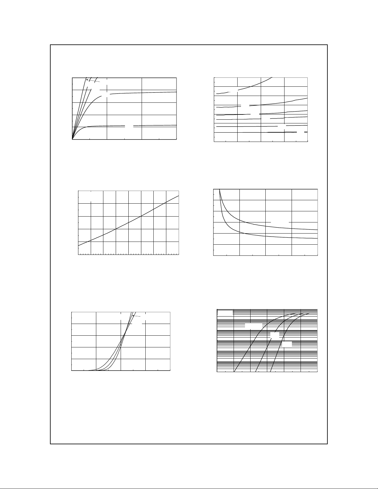
T ypical Characteristics
FDD6680A
50
40
30
20
10
, DRAIN-SOURCE CURRENT (A)
D
I
0
0123
VGS = 10V
4.5V
3.5V
3.0V
V
, DRAIN-SOURCE VOLTAGE (V)
DS
2.5V
2.2
2
VGS = 3.0V
1.8
1.6
1.4
, NORMALIZED
DS(ON)
1.2
R
1
DRAIN-SOURCE ON-RESISTANCE
0.8
0 10203040
3.5V
4.0V
4.5V
I
, DRAIN CURRENT (A)
D
Figure 1. On-Region Characteristics. Figure 2. On-Resistance Variation
with Drain Current and Gate V oltage.
1.6
ID = 14A
VGS = 10V
1.4
1.2
, NORMALIZED
1
DS(ON)
R
0.8
DRAIN-SOURCE ON-RESISTANCE
0.6
-50 -25 0 25 50 75 100 125 150
, JUNCTION TEMP E RATURE (oC)
T
J
0.03
0.025
0.02
0.015
0.01
, ON-RESISTANCE (OHM)
DS(ON)
0.005
R
0
246810
, GATE TO SOURCE VOLTAGE (V)
V
GS
TA = 125oC
TA = 25oC
6.0V
10V
ID = 7 A
Figure 3. On-Resistance Variation
with Temperature.
50
VDS = 5V
40
30
20
, DRAIN CURRENT (A)
D
I
10
0
12345
V
GS
TA = -55oC
, GATE TO SOURCE VOLTAGE (V)
25oC
125oC
Figure 4. On-Resistance Variation
with Gate-to-Source Voltage.
100
VGS = 0V
10
1
0.1
0.01
0.001
, REVERSE DRAIN CURRENT (A)
S
I
0.0001
0 0.2 0.4 0.6 0.8 1 1.2
TA = 125oC
25oC
V
, BODY DIODE FORWARD VOLTAGE (V)
SD
Figure 5. Transfer Characteristics. Figure 6. Body Diode Forward V oltage
Variation with Source Current
and Temperature.
-55oC
FDD6680A, Rev. C
 Loading...