

Fairchild Semiconductor FDD6676 Datasheet
FDD6676
30V N-Channel PowerTrench
MOSFET
FDD6676
April 2001
General Description
This N-Channel MOSFET has been designed
specifically to i mprove the overall efficiency of DC/DC
converters using either synchronous or conventional
switching PWM controllers. It has been optimized for
low gate charge, low R
extremely low R
DS( ON) and fast switching speed.
in a small package.
DS(ON)
Features
• 78 A, 30 V R
R
• Low gate charge
• Fast Switching
= 7.5 mΩ @ VGS = 10 V
DS(ON)
= 8.5 mΩ @ VGS = 4.5 V
DS(ON)
Applications
• DC/DC converter
• Motor Drives
• High performance trench te chnology for extremely
low R
DS(ON)
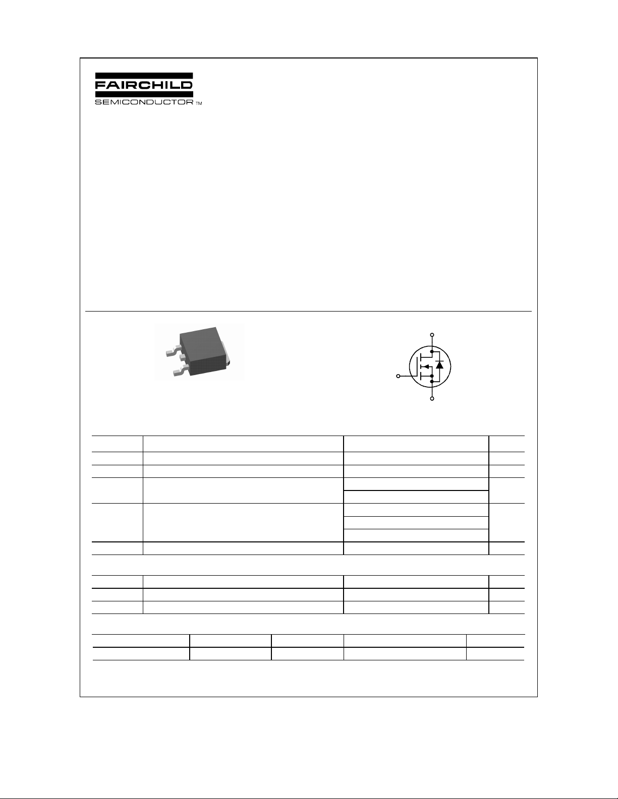
D
D
G
S
TO-252
Absolute Maximum Ratings T
o
=25
C unless otherwise noted
A
G
S
Symbol Parameter Ratings Units
V
Drain-Source Voltage 30 V
DSS
V
Gate-Source Voltage
GSS
±16
ID Drain Current – Continuous (Note 3) 78 A
– Pulsed (Note 1a) 100
PD
TJ, T
STG
Power Dissipation for Single Operation (Note 1) 83
(Note 1a)
(Note 1b)
3.8
1.6
Operating and Storage Junction Temperature Range -55 to +175
V
W
°C
Thermal Characteristics
R
θJC
R
θJA
R
θJA
Thermal Resistance, Junction-to-Case
Thermal Resistance, Junction-to-Ambient
Thermal Resistance, Junction-to-Ambient
(Note 1) 1.8
(Note 1a) 40
(Note 1b) 96
Package Marking and Ordering Information
Device Marking Device Reel Size Tape width Quantity
FDD6676 FDD6676 13’’ 12mm 2500 units
2001 Fairchild Semiconductor Corporation
°C/W
°C/W
°C/W
FDD6676 Rev C(W)
FDD6676
Electrical Characteristics T
= 25°C unless otherwise noted
A
Symbol Parameter Test Conditions Min Typ Max Units
Drain-Source Avalanche Ratings (Note 2)
W
Drain-Source Avalanche Energy Single Pulse, VDD = 15 V, ID=21A 370 mJ
DSS
IAR Drain-Source Avalanche Current 21 A
Off Characteristics
BV
Drain–Source Breakdown Voltage
DSS
∆BVDSS
∆T
I
DSS
I
GSSF
I
GSSR
Breakdown Voltage Temperature
Coefficient
J
Zero Gate Voltage Drain Current V
Gate–Body Leakage, Forward VGS = 16 V, VDS = 0 V 100 nA
Gate–Body Leakage, Reverse VGS = –16 V VDS = 0 V –100 nA
= 0 V, ID = 250 µA
V
GS
= 250 µA,Referenced to 25°C
I
D
= 24 V, VGS = 0 V 1
DS
30 V
24
mV/°C
µA
On Characteristics (Note 2)
V
Gate Threshold Voltage
GS(th)
∆VGS(th)
∆TJ
R
DS(on)
Gate Threshold Voltage
Temperature Coefficient
Static Drain–Source
On–Resistance
I
On–State Drain Current VGS = 10 V, VDS = 5 V 50 A
D(on)
= VGS, ID = 250 µA
V
DS
= 250 µA,Referenced to 25°C
I
D
VGS = 10 V, ID = 16.8 A
= 4.5 V, ID = 15.8 A
V
GS
= 10 V, ID = 16.8 A,TJ=125°C
V
GS
gFS Forward Transconductance VDS = 5 V, ID = 16.8 A 80 S
1 1.5 3 V
-5
4.8
5.4
7.3
7.5
8.5
10.5
mV/°C
mΩ
Dynamic Characteristics
C
Input Capacitance 5103 pF
iss
C
Output Capacitance 836 pF
oss
C
Reverse Transfer Capacitance
rss
V
= 15 V, V
DS
f = 1.0 MHz
= 0 V,
GS
361 pF
Switching Characteristics (Note 2)
t
Turn–On Delay Time 15 27 ns
d(on)
tr Turn–On Rise Time 9 18 ns
t
Turn–Off Delay Time 87 139 ns
d(off)
tf Turn–Off Fall Time
Qg Total Gate Charge 45 63 nC
Qgs Gate–Source Charge 13 nC
Qgd Gate–Drain Charge
V
= 15 V, ID = 1 A,
DD
V
= 10 V, R
GS
= 15V, ID = 16.8 A,
V
DS
= 5 V
V
GS
GEN
= 6 Ω
40 64 ns
12 nC
FDD6676 Rev. C(W)
 Loading...