

Fairchild Semiconductor FDD6670A Datasheet
FDD6670A
(
)
N-Channel, Logic Level, PowerTrench
MOSFET
FDD6670A
February 2000
General Description
This N-Channel Logic level MOSFET is produced using
Fairchild Semiconductor's advanced PowerTrench process
that has been especially tailored to minimize the on-state
resistance and yet maintain low gate charge for superior
switching performance.
Features
• 66 A, 30 V. R
R
DS(on)
DS(on)
= 0.008 Ω @ V
= 0.010 Ω @ V
• Low gate charge (35nC typical).
= 10 V
GS
= 4.5 V.
GS
• Fast switching speed.
Applications
• DC/DC converter
• High performance trench technology for extremely
low R
DS(on)
.
• Motor drives
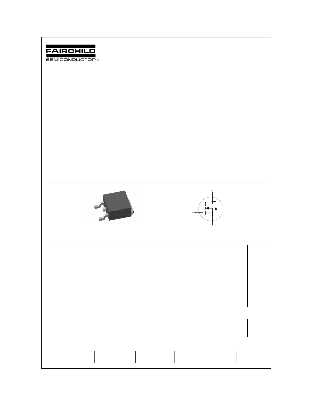
D
D
G
G
S
TO-252
=25oC unless otherwise noted
T
Absolute Maximum Ratings
Symbol Parameter Ratings Units
V
DSS
V
GSS
I
D
P
D
TJ, T
stg
Drain-Source Voltage 30 V
Gate-Source Voltage
Maximum Drain Current -Continuous
TA = 25oC
Maximum Drain Current -Pulsed 100
Maximum Power Dissipation TC = 25oC
TA = 25oC
Operating and Storage Junction Temperature Range -55 to +150
C
TA = 25oC
Note 1
(Note 1a)
(Note 1)
(Note 1a)
(Note 1b)
S
20 V
±
66
15
70
3.2
1.3
A
W
C
°
Thermal Characteristics
R
JC
θ
R
JA
θ
Thermal Resistance, Junction-to-Case
Thermal Resistance, Junction-to-Ambient
Thermal Resistance, Junction-to-Ambient
(Note 1)
(Note 1a)
(Note 1b)
1.8
40
96
Package Marking and Ordering Information
Device Marking Device Reel Size Tape width Quantity
FDD6670A FDD6670A 13’’ 16mm 2500
2000 Fairchild Semiconductor Corporation
C/W
°
C/W
°
C/W
°
FDD6670A, Rev. C
Electrical Characteristics
TA = 25°C unless otherwise noted
Symbol Parameter Test Conditions Min Typ Max Units
FDD6670A
Drain-Source Avalanche ratings
W
DSS
I
AR
Single Pulse Drain-Source
Avalanche Energy
Maximum Drain-Source Av alanche Current 66 A
Off Characteristics
BV
DSS
DSS
BV
∆
T
J
∆
I
DSS
I
GSSF
I
GSSR
On Characteristics
V
GS(th)
GS(th)
V
∆
T
J
∆
R
DS(on)
I
D(on)
g
FS
Drain-Source Breakdown
Voltage
Breakdown Voltage
Temperature Coefficient
Zero Gate Voltage Drain
Current
Gate-Body Leakage Current,
Forward
Gate-Body Leakage Current,
Reverse
(Note 2)
Gate Threshold Voltage VDS = VGS, ID = 250 µA11.63V
Gate Threshold Voltage
Temperature Coefficient
Static Drain-Source
On-Resistance
On-State Drain Current VGS = 10 V, VDS = 5 V 50 A
Forward Transconductance VDS = 5 V, ID = 12 A 55 S
Dynamic Characteristics
C
iss
C
oss
C
rss
Input Capacitance 3200 pF
Output Capacitance 820 pF
Reverse Transfer Capacitance
(Note 2)
VDD = 15 V, ID = 66 A 400 mJ
VGS = 0 V, ID = 250 µA30 V
ID = 250 µA, Referenced to 25°C25mV/
VDS = 24 V, VGS = 0 V 1
C
°
A
µ
VGS = 20V, VDS = 0 V 100 nA
VGS = -20 V, VDS = 0 V -100 nA
ID = 250 µA, Referenced to 25°C-4mV/
VGS = 10 V, ID = 15 A
V
= 10 V, ID = 15 A,TJ=125°C
GS
V
= 4.5 V, ID =13 A
GS
= 15 V, VGS = 0 V,
V
DS
0.0065
0.0090
0.0085
0.008
0.013
0.010
C
°
Ω
f = 1.0 MHz
400 pF
(Note 2)
Switching Characteristics
t
d(on)
t
r
t
d(off)
t
f
Q
Q
Q
g
gs
gd
Turn-On Delay Time 15 27 ns
Turn-On Rise Time 15 27 ns
Turn-Off Delay Time 85 105 ns
Turn-Off Fall Time
Total Gate Charge 35 50 nC
Gate-Source Charge 9 nC
Gate-Drain Charge
= 15 V, ID = 1 A,
V
DD
= 10 V, R
V
GS
V
= 15 V, ID = 15 A,
DS
= 5 V,
V
GS
GEN
= 6
Ω
Drain-Source Diode Characteristics and Maximum Ratin gs
I
S
V
SD
Notes:
1. R
is the sum of the junction-to-case and case-to-ambient resistance where the case thermal reference is defined as the drain tab.
θJA
R
is guaranteed by design while R
θJC
Scale 1 : 1 on letter size paper
2. Pulse Test: Pulse Width ≤ 300 µs, Duty Cycle ≤ 2.0%
Maximum Continuous Drain-Sourc e Diode Fo rward Current 2.3 A
Drain-Source Diode Forward
VGS = 0 V, IS = 2.3 A
(Note 2)
Voltage
is determined by the user's board design.
θCA
b) R
a) R
= 40oC/W when mounted
θJA
on a 1in2 pad of 2oz copper.
= 96oC/W when mounted
θJA
on a minimum pad .
42 68 ns
16 nC
0.72 1.2 V
FDD6670A, Rev. C
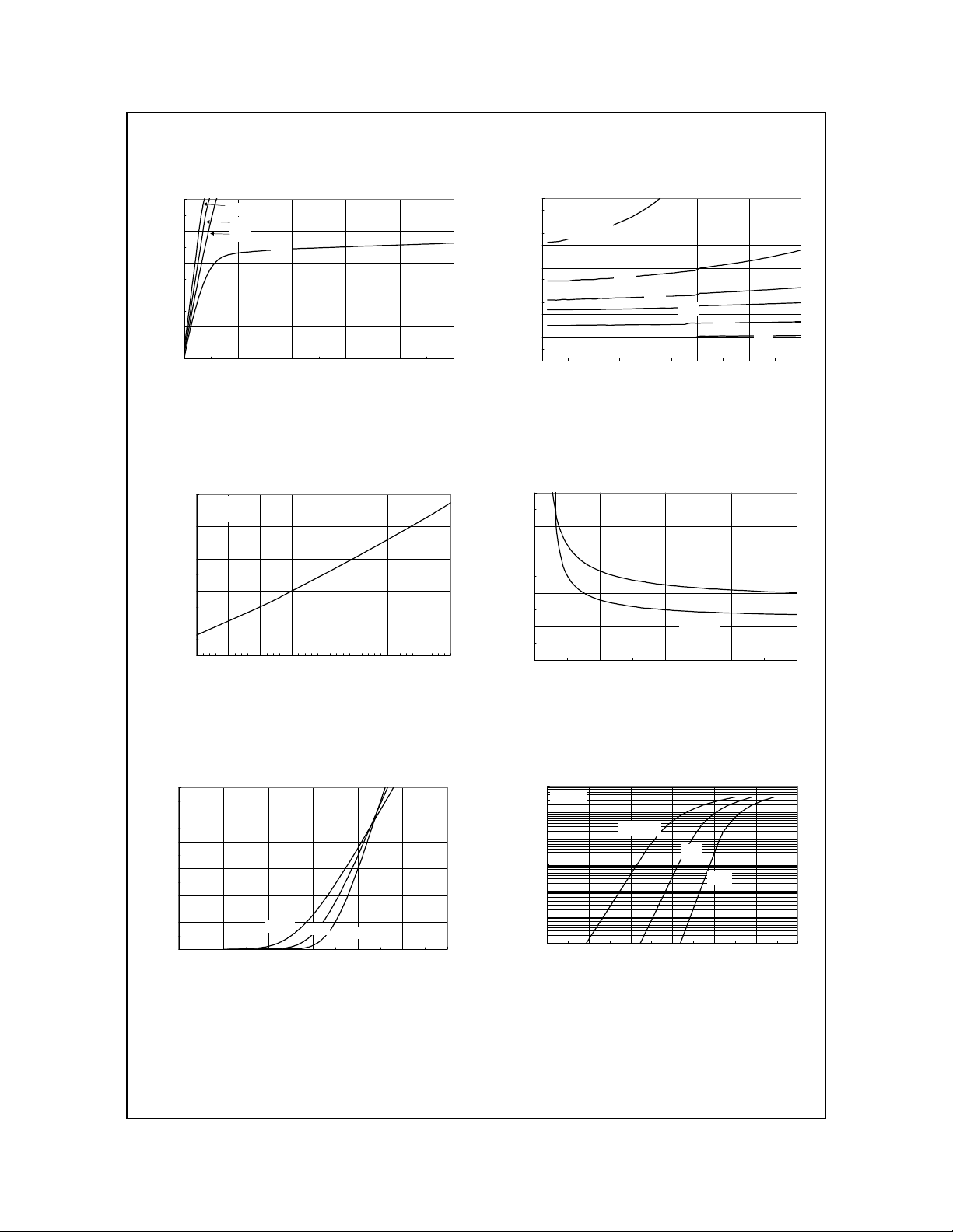
T ypical Characteristics
T=-55oC
25oC
FDD6670A
50
40
30
20
10
, DRAIN-SOURCE CURRENT (A)
D
I
0
VGS = 10V
4.5V
3.5V
3.0V
012345
V
, DRAIN-SOURCE VOLTAGE (V)
DS
Figure 1. On-Region Characteristics.
1.6
ID = 15A
VGS = 10V
1.4
1.2
, NORMALIZED
1
DS(ON)
R
0.8
DRAIN-SOURCE ON-RESISTANCE
0.6
-50 -25 0 25 50 75 100 125 150
, JUNCTION TEMPERATURE (oC)
T
J
2.2
2
VGS = 3.0V
1.8
1.6
1.4
, NORMALIZED
DS(ON)
1.2
R
1
DRAIN-SOURCE ON-RESISTANCE
0.8
0 1020304050
3.5V
4.0V
I
, DRAIN CURRENT (A)
D
4.5V
6.0V
10V
Figure 2. On-Resistance Variation
with Drain Current and Gate Voltage.
0.025
ID = 8 A
0.02
0.015
0.01
, ON-RESISTANCE (OHM)
0.005
DS(ON)
R
0
246810
V
, GATE TO SOU R CE VOLTAGE ( V)
GS
TA = 125oC
TA = 25oC
Figure 3. On-Resistance Variation
with Temperature.
60
VDS = 5V
50
40
30
20
, DRAIN CURRENT (A)
D
I
10
0
11.522.533.54
125oC
, GATE TO SOURCE VOLTAGE (V)
V
GS
Figure 5. Transfer Characteristics.
Figure 4. On-Resistance Variation
with Gate-to-Source Voltage.
100
VGS = 0V
10
1
0.1
0.01
0.001
, REVERSE DRAIN CURRENT (A)
S
I
0.0001
0 0.2 0.4 0.6 0.8 1 1.2
TA = 125oC
25oC
-55oC
, BODY DIODE FORWARD VOLTAGE (V)
V
SD
Figure 6. Body Diode Forward V oltage
Variation with Source Current
and Temperature.
FDD6670A, Rev. C
 Loading...