

Fairchild Semiconductor FDD6630A Datasheet
FDD6630A
N-Channel PowerTrenchTM MOSFET
FDD6630A
July 1999
ADVANCE INFORMATION
General Description
This N-Channel Logic level MOSFET is produced using
Fairchild Semiconductor's advanced PowerTrench
process that has been especially tailored to minimize
Features
21 A, 30 V. R
R
= 0.035 Ω @ V
DS(ON)
= 0.050 Ω @ V
DS(ON)
= 10 V
GS
= 4.5 V.
GS
the on-state resistance and yet maintain low gate
charge for superior switching performance.
Applications
DC/DC converter
Motor drives
Low gate charge.
Fast switching speed.
High performance trench technology for extremely
low R
DS(ON)
.
D
D
G
G
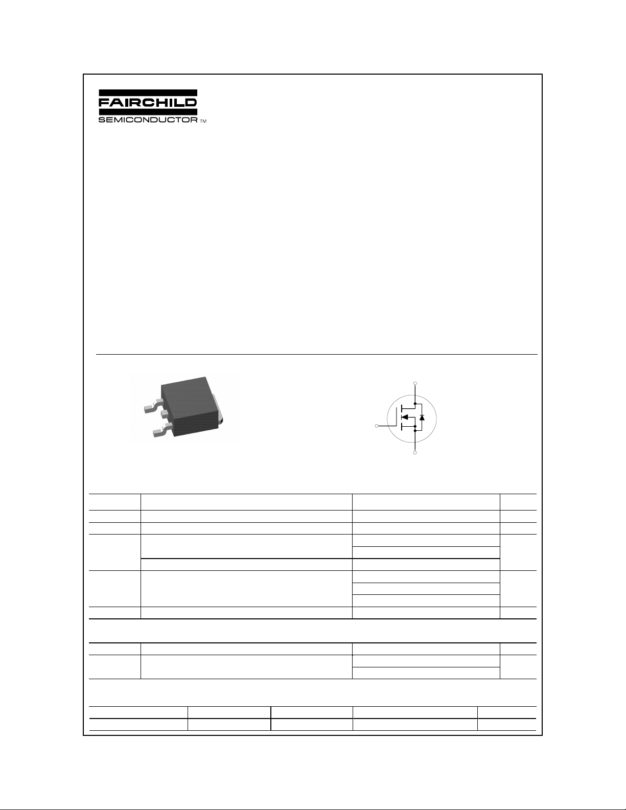
S
TO-252
Absolute Maximum Ratings
Symbol Parameter Ratings Units
V
DSS
V
GSS
I
D
P
D
TJ, T
stg
Drain-Source Voltage 30 V
Gate-Source Voltage
Maximum Drain Current -Continuous
(N o te 1 a )
Maximum Drain Current -Pulsed 100
Maximum P ower Dissipation @ TC = 25oC
TA = 25oC
Operating and Storage Junction Temperature Range -55 to +150
TC=25oC unless otherwise noted
(Note 1)
(Note 1)
TA = 25oC
(Note 1 a )
(Note 1 b )
S
±20
21
7.6
28
3.2
1.3
V
A
W
°
C
Thermal Characteristics
R
JC
θ
R
JA
θ
Therm a l Re sis tan c e, J un ctio n-to - Ca se
Thermal Resistance, Junction-to- Ambient
(N o te 1 b )
(Note 1)
(Note 1a)
4.5
40
96
Package Marking and Ordering Information
Device Marking Device Reel Size Tape Width Quantity
FDD6630A FDD6630A 13’’ 16m m 2500
1999 Fairchild Semiconductor Corporation
°C/W
°
C/W
°C/W
FDD6630A Rev. A
FDD6630A
Electrical Characteristics T
=25oC unless otherwise noted
C
Symbol Parameter Test Conditions Min Typ Max Units
OFF CHARACTERISTICS
BV
I
DSS
I
GSSF
I
GSSR
DSS
Drain-Source Breakdown Voltage
= 0 V, ID = 250 µA
V
GS
Zero Gate Voltage Drain Current VDS = 24 V, VGS = 0 V 1
Gate-Body Leakage, Forward VGS = 20 V, VDS = 0 V 100 nA
Gate-Body Leakage, Reverse VGS = -20 V, VDS = 0 V -100 nA
30 V
µA
ON CHARACTERISTICS (Note 2)
V
GS(TH)
R
DS(ON)
Gate Threshold Voltage
Static Drain-Sourc e
On-Resistance
= VGS, ID = 250 µA
V
DS
VGS = 10 V, ID = 7.6 A
V
= 4.5 V, ID = 6.3 A
GS
13V
0.035
Ω
0.050
DRAIN-SOURCE DIODE CHARACTERISTICS AND MAXIMUM RATINGS
I
S
V
SD
Notes:
1. R
R
θJC
θJA
Maximum Continuous Drain-S ource Diode Forward Current 21 A
Drain-Source Diode Forward
VGS = 0 V, IS = 2.7 A 1.2 V
Voltage
is the sum of the junction-to-case and case-to-ambient thermal resistance where the case thermal reference is defined as the drain tab.
is guaranteed by design while R
is determined by the user's board design. R
θCA
a) R
= 40oC/W when mounted on a
θJA
1 in2 pad of 2oz copper.
has been used to determine some maximum ratings.
θJC
b) R
= 96oC/W when mounted on
θJA
minimum pad.
Scale 1 : 1 on letter size paper
2. Pulse Test: Pulse Width ≤ 300 µs, Duty Cycle ≤ 2.0%
FDD6630A Rev. A
 Loading...