

Fairchild Semiconductor FDD603AL Datasheet
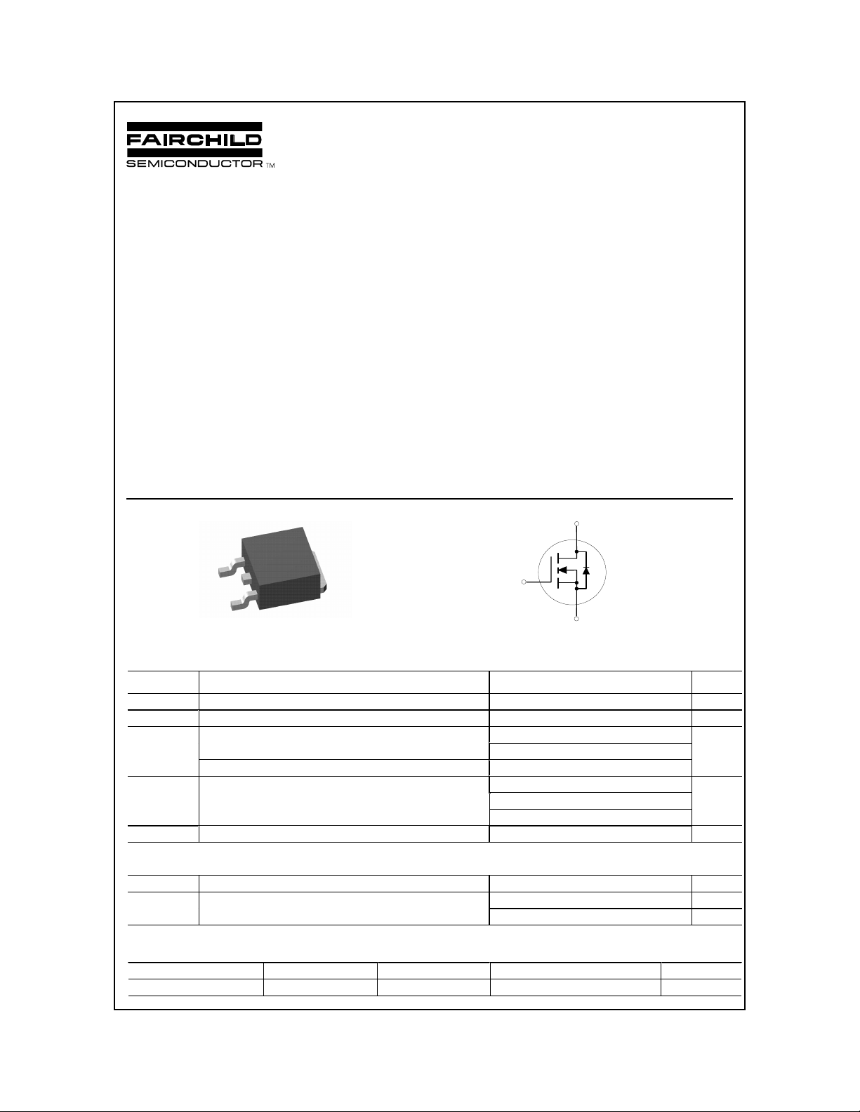
FDD603AL
N-Channel Logic Level Enhancement Mode Field Effect Transistor
FDD603AL
July 1999
General Description
This N-Channel logic level enhancement mode power
field effect transistor is produced using Fairchilds
proprietary, high cell density, DMOS technology. This
Features
33 A, 30 V. R
R
= 0.023 Ω @ V
DS(ON)
= 0.037 Ω @ V
DS(ON)
= 10 V
GS
= 4.5 V.
GS
very high density process is tailored to minimize onstate resistance. These devices are particularly suited
for low voltage applications such as DC/DC converters
and high efficiency switching circuits where fast
switching, low in-line power loss, and resistance to
transients are needed.
Applications
Critical DC electrical parameters specified at elevated
temperature.
Rugged avalanche-rated internal source-drain diode
can eliminate the need for external Zener Diode.
High density cell design for extremely low R
DS(ON)
.
DC/DC converters
Motor drives
D
D
G
G
S
TO-252
Abso lu te Maxim u m R a tin g s
Symbol Parameter Ratings Units
V
DSS
V
GSS
I
D
P
D
TJ, T
stg
Drain-Source Voltage 30 V
Gate-Source Voltage
Maximum Drain Current - Continuous
Maximum Drain Current -Pulsed 80
Maximum P ower Dissipation @ TC = 25oC
TA = 25oC
Operating and Storage Junction Temperature Range -55 to +150
TC=25oC unless otherwise noted
(Note 1)
= 25°C
(Note 1 a )
(Note 1)
(Note 1a)
(Note 1b)
T
A
TA = 25oC
S
±20
33
9.5
39
3.2
1.3
V
A
W
°C
Thermal Characteristics
R
JC
θ
R
JA
θ
Thermal Resistance, Junction-to-Case
Thermal Resistance, Junction-to-Ambient
(No te 1 b )
(Note 1)
(Note 1a)
2.5
40
96
Package Marking and Ordering Information
Device Marking Device Reel Size Tape Width Quantity
FDD603AL FDD603AL 13’’ 16mm 2500
1999 Fairchild Semiconductor Corporation
°
C/W
°C/W
°C/W
FDD603AL, Rev. B
FDD603AL
Electrical Characteristics T
= 25°C unless otherwise noted
A
Symbol Parameter Test Conditions Min Typ Max Units
Off Characteristics
W
DSS
I
AR
BV
DSS
∆BVDSS
∆T
I
DSS
I
GSSF
I
GSSR
Single Pulse Drain-Source
VDD = 15 V, ID = 12 A 100 mJ
Avalanche Energy
Maximum Drain-Source Avalanche Current 12 A
Drain-Source Breakdown Voltage
Breakdown Voltage Temperature
Coefficient
J
= 0 V, ID = 250 µA
V
GS
= 250µA, Referenced to 25°C
I
D
30 V
32
Zero Gate Voltage Drain Current VDS = 24 V, VGS = 0 V 10
Gate-Body Leakage Current,
VGS = 20V, VDS = 0 V 100 nA
Forward
Gate-Body Leakage Current,
VGS = -20 V, VDS = 0 V -100 nA
Reverse
mV/°C
µA
On Characteristics (Note 2)
V
GS(th)
∆VGS(th)
∆T
J
R
DS(on)
I
D(on)
g
FS
Gate Threshold Voltage
Gate Threshold Voltage
Temperature Coefficient
Static Drain-Source
On-Resistance
= VGS, ID = 250 µA
V
DS
= 250 µA,Referenced to 25°C
I
D
VGS = 10 V, ID = 9.5 A
V
= 10 V, ID = 9.5 A,TJ=125°C
GS
V
= 4.5 V, ID = 7.5 A
GS
On-State Drain Current VGS = 10 V, VDS = 10 V 60 A
Forward Transconductance VDS = 10 V, ID = 9.5 A 18 S
11.7 3 V
-4.5
0.016
0.024
0.026
0.023
0.035
0.037
mV/°C
Ω
Dynamic Characteristics
C
iss
C
oss
C
rss
Input Capacitance 670 pF
Output Capacitance 345 pF
Reverse Transfer Capacitance
V
= 15 V, VGS = 0 V
DS
f = 1.0 MHz
95 pF
Switching Characteristics (Note 2)
t
d(on)
t
r
t
d(off)
t
f
Q
Q
Q
g
gs
gd
Turn-On Delay Time 10 20 ns
Turn-On Rise Time 16 30 ns
= 15 V, ID = 1 A
V
DD
V
= 10 V, R
GS
GEN
= 6 Ω
Turn-Off Delay Time 27 45 ns
Turn-Off Fall Time
Total Gate Charge 19 26 nC
Gate-Source Charge 3.5 nC
V
=10 V, ID = 9.5 A
DS
= 10 V,
V
GS
Gate-Drain Charge
12 22 ns
5.5 nC
Drain-Source Diode Characteristics and Maximum Ratings
I
S
V
SD
Notes:
1. R
θJA
R
Scale 1 : 1 on letter size paper
2. Pulse Test: Pulse Width ≤ 300 µs, Duty Cycle ≤ 2.0%
Maximum Continuous Drain-Source Diode Forward Current ( Note 1) 33 A
Drain-Source Diode Forward
VGS = 0 V, IS = 2.3 A (Note 2) 0.78 1.2 V
Voltage
is the sum of the junction-to-case and case-to-ambient thermal resistance where the case thermal reference is defined as the drain tab.
is guaranteed by design while R
θJC
is determined by the user's board design. R
θCA
a) R
= 40oC/W when mounted
θJA
on a 1in2 pad of 2oz copper.
has been used to determine some maximum ratings.
θJC
b) R
= 96oC/W on a minimum
θJA
mounting pad.
FDD603AL, Rev. B
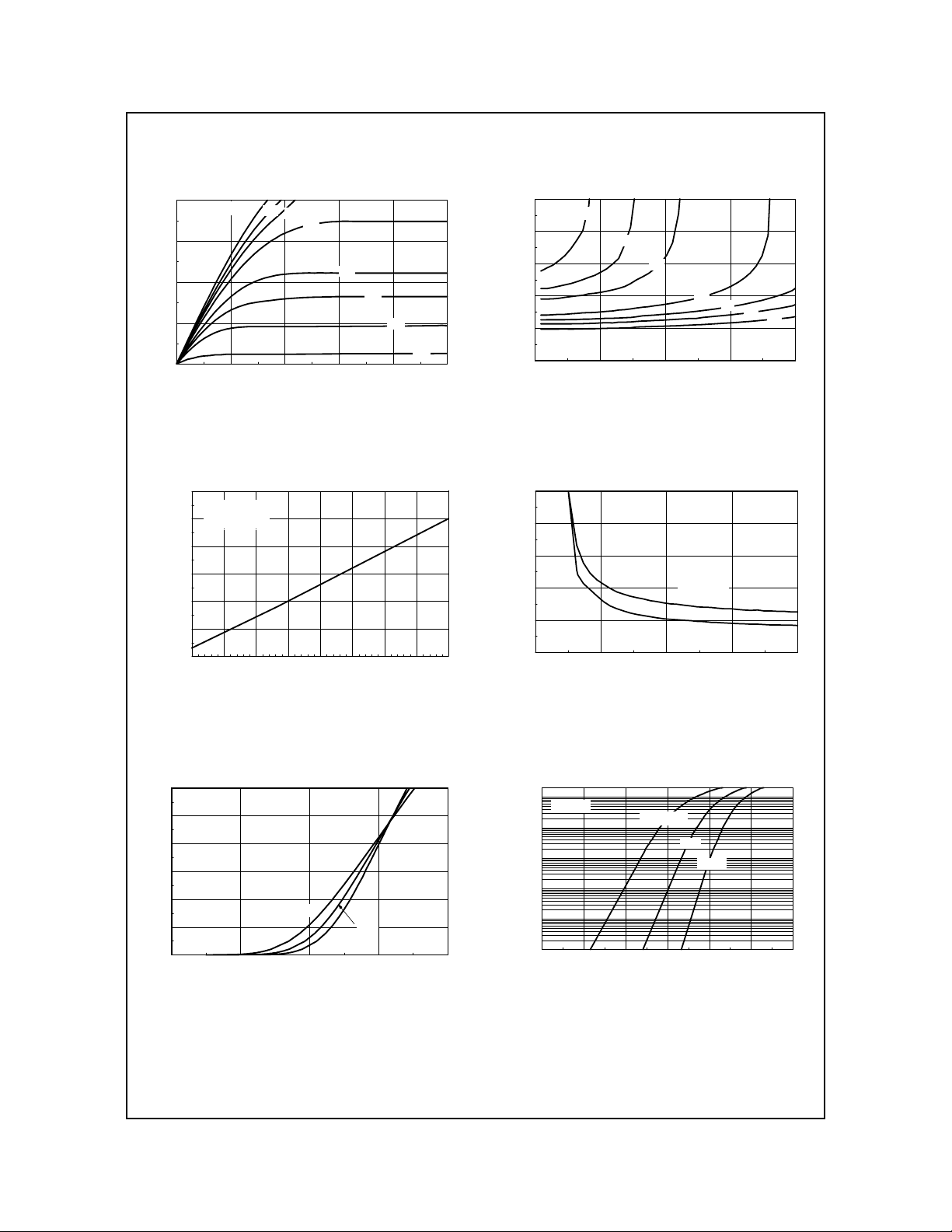
Typical Characteristics
FDD603AL
80
V =10V
GS
60
40
8.0
7.0
6.0
5.0
4.5
20
D
I , DRAIN-SOURCE CURRENT (A)
0
012345
V , DRAIN-SOURCE VOLTAGE (V)
DS
4.0
3.0
3
V = 4.0V
GS
2.5
2
1.5
DS(ON)
R , NORMALIZED
1
DRAIN-SOURCE ON-RE SISTANCE
0.5
0 20406080
4.5
5.0
I , DRAIN CURRENT (A)
D
Figure 1. On-Region Characteristics. Figure 2. On-Resistance Variation
with Drain Current and Gate Voltage.
1.8
I = 9.5A
D
1.6
V = 10V
GS
1.4
1.2
1
DS(ON)
R , NORMALIZED
0.8
DRAIN-SOURCE ON-RESISTANCE
0.6
-50 -25 0 25 50 75 100 125 150
T , JUNCTION TEMPERATURE (°C)
J
0.1
0.08
0.06
T = 125°C
0.04
0.02
DS(ON)
R , ON-RESISTANCE (OHM)
0
246810
V , GATE TO SOURCE VOLTAGE (V)
GS
J
6.0
25°C
7.0
8.0
I = 5A
D
10
Figure 3. On-Resistance Variation
with Temperature.
30
V = 10V
DS
25
20
15
10
D
I , DRAIN CURRENT (A)
5
0
12345
T = 125°C
J
25°C
-55°C
V , GATE TO SOURCE VOLTAGE (V)
GS
Figure 4. On-Resistance Variation
with Gate-to-Source Voltage.
20
V = 0V
GS
1
0.1
0.01
0.001
S
I , REVERSE DRAIN CURRENT (A)
0.0001
0 0.2 0.4 0.6 0.8 1 1.2
V , BODY DIODE FORWARD VOLTAGE (V)
SD
T = 125°C
J
Figure 5. Transfer Characteristics. Figure 6. Body Diode Forward Voltage
Variation with Source Current
and Temperature.
25°C
-55°C
FDD603AL, Rev. B
 Loading...