

Fairchild Semiconductor FDD6030L Datasheet
ADVANCE INFORMA TION
(
)
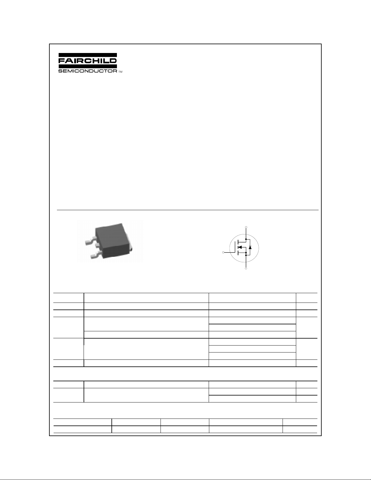
FDD6030L
N-Channel Logic Level Enhancement Mode Field Effect Transistor
FDD6030L
July 1999
General Description
These N-Channel logic level enhancement mode power
field effect transistors are produced using Fairchild’s
proprietary, high cell density, DMOS technology. This
Features
• 50 A, 30 V. R
R
= 0.0135 Ω @ V
DS(ON)
= 0.0200 Ω @ V
DS(ON)
= 10 V
GS
= 4.5 V.
GS
very high density process is especially tailored to
minimize on-state resistance. These devices are
particularly suited for low voltage applications such as
DC/DC converters and high efficiency switching circuits
where fast switching, low in-line power loss, and
resistance to transients are needed.
• Low gate charge.
• Fast switching speed.
• Low Crss.
D
D
G
G
S
TO-25 2
T
=25oC unless otherwise noted
Ab s o lute Maximum Ratin g s
Symbol Parameter Ratings Units
V
DSS
V
GSS
I
D
P
D
TJ, T
stg
Drain-Source Voltage 30 V
Gate-Source Voltage
Maximum Drain Current -Continuous
Maximum Drain Current -Pulsed 150
Maximum Power Dissipation @ TC = 25oC
TA = 25oC
Operating and Storage Junction Temperature Range -55 to +150
C
TA = 25oC
Note 1
(Note 1a)
(Note 1)
(Note 1 a )
(Note 1 b )
S
20 V
±
50
12
60
3.2
1.3
A
W
C
°
Thermal Characteristics
R
JC
θ
JA
θ
Therma l Res ista nc e, J u nc tion-to- C as e
Thermal Resistance, Junction-to- Ambient
(Note 1b)
(Note 1)
(Note 1a)
2.1
39
96
Package Marking and Ordering Information
Device Marking Device Reel Size Tape width Quantity
FDD6030L FDD6030L 13’’ 16m m 2500
1999 Fairchild Semiconductor Corporation
C/W
°
C/WR
°
C/W
°
FDD6030L Rev. A1
FDD6030L
Electrical Characteristics
TC=25oC unless otherwise noted
Symbol Parameter Test Conditions Min Typ Max Units
OFF CHARACTERISTICS
BV
DSS
I
DSS
I
GSSF
I
GSSR
ON CHARACTERISTICS
V
GS(TH)
R
DS(ON)
Drain-Source Breakdown Voltage VGS = 0 V, ID = 250 µA30 V
Zero Gate Voltage Drain Current VDS = 24 V, VGS = 0 V 10
µ
Gate-Body Leakage, Forward VGS = 20 V, VDS = 0 V 100 nA
Gate-Body Leakage, Reverse VGS = -20 V, VDS = 0 V -100 nA
(Note 2)
Gate Threshold Voltage VDS = VGS, ID = 250 µA1 3V
Static Drain-Source
On-Resistance
VGS = 10 V, ID = 12 A
V
= 4.5 V, ID = 10 A
GS
0.0135
0.0200
DRAIN-SOURCE DIODE CHARACTERISTICS AND MAXIMUM RATINGS
I
S
V
SD
Notes:
1. R
R
θJC
θJA
Maximum Continuous Drain-Source Diode Forward Current
Drain-Source Diode Forward
VGS = 0 V, IS = 2.7 A
Voltage
is the sum of the junction-to-case and case-to-ambient thermal resistance where the case thermal reference is defined as the drain tab.
is guaranteed by design while R
is determined by the user's board design.
θCA
a) R
= 40oC/W when mounted on a
θJA
1 in2 pad of 2oz copper.
1.2 V
b) R
= 96oC/W when mounted on
θJA
a 0.076 in2 pad of 2oz copper.
2.7 A
A
Ω
Scale 1 : 1 on letter size paper
2. Pulse Test: Pulse W idth ≤ 300 µs, Duty Cycle ≤ 2.0%
FDD6030L Rev. A1
 Loading...