

Fairchild Semiconductor FDD5690 Datasheet
FDD5690
60V N-Channel PowerTrenchTM MOSFET
FDD5690
June 1999
PRELIMINARY
General Description
This N-Channel MOSFET has been designed specifically
to improve the overall efficiency of DC/DC converters using
either synchronous or conventional switching PWM
controllers.
These MOSFETs feature faster switching and lower gate
charge than other MOSFETs with comparable R
specifications.
DS(ON)
Features
30 A, 60 V. R
R
DS(ON)
DS(ON)
= 0.027Ω @ V
= 0.032 Ω @ V
= 10 V
GS
= 6 V.
GS
Low gate charge (23nC typical).
Fast switching speed.
High performance trench technology for extremely
low R
DS(ON)
.
The result is a MOSFET that is easy and safer to drive
(even at very high frequencies), and DC/DC power supply
designs with higher overall efficiency.
D
D
G
G
S
TO-252
Absolute Maximum Ratings
Symbol Parameter Ratings Units
V
DSS
V
GSS
I
D
P
D
TJ, T
stg
Drain-Source Voltage 60 V
Gate-Source Voltage
Maximum Dra in Cu rrent -C on tinuo u s
(Note 1 a )
Maximum Drain Current -Pulsed 100
Maximum Power Dissipation @ TC = 25oC
TA = 25oC
Operating and Storage Junction Temperature Range -55 to +150
TC=25oC unless otherwise noted
(Note 1)
(Note 1)
TA = 25oC
(Note 1a )
(Note 1b )
S
±20
30
9
50
3.2
1.3
V
A
W
°C
Thermal Characteristics
R
JC
θ
R
JA
θ
Therm al R es is tan ce , Ju nc tion -to- C as e
Thermal Resistance, Junction-to- Ambient
(Note 1 b )
Package Marking and Ordering Inform ation
Device Marking Device Reel Size Tape width Quantity
FDD5690 FDD5690 13’’ 16mm 2500
1999 Fairchild Semiconductor Corporation
(Note 1)
(Note 1a)
2.5
40
96
°
C/W
°C/W
°C/W
FDD5690, Rev. B
FDD5690
Electrical Characteristics T
= 25°C unless otherwise noted
A
Symbol Parameter Test Conditions Min Typ Max Units
Off Characteristics
W
DSS
I
AR
BV
DSS
∆BVDSS
∆T
J
I
DSS
I
GSSF
I
GSSR
Single Pulse Drain-Source
VDD = 30 V, ID = 30 A 90 mJ
Avalanche Energy
Maximum Drain-Source Avalanche Current 30 A
Drain-Source Breakdown Voltage
Breakdown Voltage Temperature
Coefficient
= 0 V, ID = 250 µA
V
GS
= 250µA, Referenced to 25°C
I
D
60 V
57
mV/°C
Zero Gate Voltage Drain Current VDS = 48 V, VGS = 0 V 1
Gate-Body Leakage Current,
VGS = 20V, VDS = 0 V 100 nA
Forward
Gate-Body Leakage Current,
VGS = -20 V, VDS = 0 V -100 nA
Reverse
µA
On Characteristics (Note 2)
V
GS(th)
∆VGS(th)
∆T
J
R
DS(on)
I
D(on)
g
FS
Gate Threshold Voltage
Gate Threshold Voltage
Temperature Coefficient
Static Drain-Source
On-Resistance
= VGS, ID = 250 µA
V
DS
= 250 µA,Referenced to 25°C
I
D
VGS = 10 V, ID = 9 A
V
= 10 V, ID = 9 A, TJ = 125°C
GS
V
= 6 V, ID = 8 A
GS
On-State Drain Current VGS = 10 V, VDS = 5 V 25 A
Forward Transconductance VDS = 5 V, ID = 9 A 24 S
22.54 V
-6
0.023
0.032
0.026
0.027
0.048
0.032
mV/°C
Ω
Dynamic Characteristics
C
iss
C
oss
C
rss
Input Capacitance 1110 pF
Output Capacitance 150 pF
Reverse Transfer Capacitance
V
= 25 V, VGS = 0 V
DS
f = 1.0 MHz
75 pF
Switching Characteristics (Note 2)
t
d(on)
t
r
t
d(off)
t
f
Q
Q
Q
g
gs
gd
Turn-On Delay Time 10 18 ns
Turn-On Rise Time 9 18 ns
= 30 V, ID = 1 A
V
DD
V
= 10 V, R
GS
GEN
= 6 Ω
Turn-Off Delay Time 24 39 ns
Turn-Off Fall Time
Total Gate Charge 23 32 nC
Gate-Source Charge 4 nC
V
= 30 V, ID = 9 A
DS
= 10 V,
V
GS
Gate-Drain Charge
Drain-Source Diode Characteristics and Maximum Ratings
I
S
V
SD
Notes:
1. R
is the sum of the junction-to-case and case-to-ambient thermal resistance where the case thermal reference is defined as the drain tab.
θJA
R
θJC
Scale 1 : 1 on letter size paper
2. Pulse Test: Pulse Width ≤ 300 µs, Duty Cycle ≤ 2.0%
Maximum Continuous Drain-Source Di ode Forward Current 2.3 A
Drain-Source Diode Forward
VGS = 0 V, IS = 2.3 A (Note 2) 0.75 1.2 V
Voltage
is guaranteed by design while R
is determined by the user's board design.
θCA
a) R
= 40oC/W when mounted
θJA
on a 1in2 pad of 2oz copper.
b) R
= 96oC/W on a minimum
θJA
mounting pad.
10 18 ns
6.8 nC
FDD5690, Rev. B
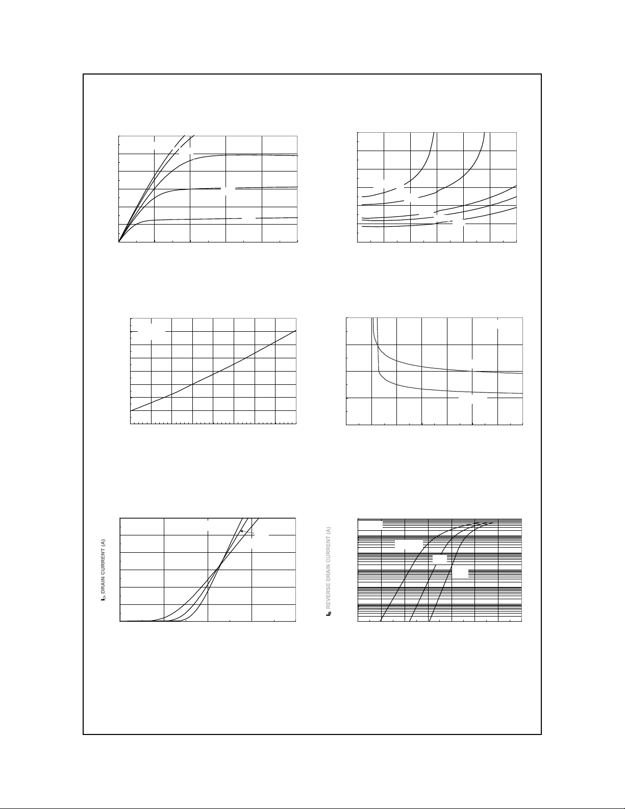
Typical Characteristics
6.0V
FDD5690
60
50
40
30
20
10
, DRAIN-SOURCE CURRENT (A)
D
I
0
VGS = 10V
5.0V
4.5V
4.0V
012345
V
, DRAIN-SOURCE VOLTAGE (V)
DS
Figure 1. On-Region Characteristics.
2
ID = 9A
1.8
= 10V
V
GS
1.6
1.4
1.2
, NORMALIZED
1
DS(ON)
R
0.8
0.6
DRAIN-SOURCE ON-RESISTANCE
0.4
-50 -25 0 25 50 75 100 125 150
, JUNCTION TEMPERATURE (oC)
T
J
2
1.8
1.6
VGS = 4.5V
1.4
, NORMALIZED
1.2
DS(ON)
R
1
DRAIN-SOURCE ON-RESISTANCE
0.8
0 102030405060
5.0V
I
, DRAIN CURRENT (A)
D
Figure 2. On-Resistance Variation
with Drain Current and Gate Voltage.
0.08
0.06
0.04
, ON-RESISTANCE (OHM)
0.02
DS(ON)
R
0
345678910
, GATE TO SOURCE VOLTAGE (V)
V
GS
TA = 125oC
TA = 25oC
ID = 15A
Figure 3. On-Resistance Variation
with Temperature.
60
VDS = 5V
50
40
30
20
10
0
23456
V
, GATE TO SOURCE VOLTAGE (V)
GS
TA = -55oC
25oC
125oC
Figure 4. On-Resistance Variation
with Gate-to-Source Voltage.
100
VGS = 0V
10
1
0.1
0.01
0.001
0.0001
0 0.2 0.4 0.6 0.8 1 1.2 1.4
TA = 125oC
25oC
-55oC
, BODY DIODE FORWARD VOLTAGE (V)
V
SD
Figure 5. Transfer Characteristics. Figure 6. Body Diode Forward Voltage
Variation with Source Current
and Temperature.
FDD5690, Rev. B
 Loading...