

Fairchild Semiconductor FDD3672 Datasheet
FDD3672
N-Channel UltraFET® Trench MOSFET
100V, 44A, 28mΩ
FDD3672
June 2002
Features
•r
•Q
• Low Miller Charge
= 24mΩ (Typ.), V
DS(ON)
(tot) = 24nC (Typ.), V
g
= 10V, ID = 44A
GS
= 10V
GS
Applications
• DC/DC converters and Off-Line UPS
• Distributed Power Architectures and VRMs
• PrimarySwitch for 24V and 48V Systems
• Low Qrr Body Diode
• Optimized eff iciency at high frequ encies
• UIS Capability (Single Pulse and Repetitive Pulse)
• Qualified to AEC Q101
• High Voltage Synchronous R ectifier
• Direct Injection / Diesel Injection System
• 42V Automotive Load Control
• Electronic Valve Train System
Formerly developmental type 82760
GATE
SOURCE
DRAIN
(FLANGE)
G
D
TO-252AB
FDDSERIES
MOSFET Maximum Ratings T
= 25°C unless otherwise noted
C
Symbol Parameter Ratings Units
V
DSS
V
GS
Drain to Source Voltage 100 V
Gate to Source Voltage ±20 V
Drain Curr e nt
Continuous (T
I
D
Continuous (T
Continuous (T
= 25oC, VGS = 10V)
C
= 100oC, VGS = 10V) 31 A
C
= 25oC, VGS = 10V, R
amb
= 52oC/W) 6.5 A
θJA
Pulsed Figure 4 A
E
AS
P
D
, T
T
J
STG
Single Pulse Avalanche Energy (Note 1) 120 mJ
Power dissipation 135 W
Derate above 25
o
C0.9W/
Operating and Storage Temperature -55 to 175
S
44 A
o
C
o
C
Thermal Characteristics
R
θJC
R
θJA
R
θJA
This product ha s been des igned to me et the e xtr eme test c ondit ions and envir onment deman ded by the automot ive indus t ry. For a
All Fairchild Semiconductor prod ucts are manufactured, assembled and tested under ISO9000 and QS9000 quality systems
©2002 Fairchild Semiconductor Corporation
Thermal Resistance Junction to Case TO-252 1.11
Thermal Resistance Junction to Ambient TO-252 100
Thermal Resistance Junction to Ambient TO-252, 1in2 copper pad ar ea 52
copy of the requirements, see AEC Q101 at: http://www.aecouncil.com/
Reliability data can be found at: http://www.fairchildsemi.com/products/discrete/reliability/index.html.
certification.
FDD3672 Rev. A
o
C/W
o
C/W
o
C/W

Package Marking and Ordering Information
Device Marking Device Package Reel Size Tape Width Quantity
FDD3672 FDD3672 TO-252AA 330mm 16mm 2500 units
FDD3672
Electrical Characteristics
TC = 25°C unless otherwise noted
Symbol Parameter Test Conditions Min Typ Max Units
Off Characteristics
B
I
DSS
I
GSS
VDSS
Drain t o Source Breakdown Volta ge ID = 250µA, VGS = 0V 100 - - V
V
= 80V - - 1
Zero Gate Voltage Drain Current
DS
= 0V TC= 150oC- - 250
V
GS
Gate to Source Leakage Current VGS = ±20V - - ±100 nA
On Characteristics
V
GS(TH)
r
DS(ON)
Gate to Source Threshold Voltage VGS = VDS, ID = 250µA2-4V
I
Drain to Source On Resistance
= 44A, V
D
= 21A, VGS = 6V, - 0.031 0.047
D
I
=44A, VGS=10V, TC=175oC - 0.054 0.068
D
= 10V - 0.024 0.028
GS
Dynamic Characteristics
C
C
C
Q
Q
Q
Q
Q
ISS
OSS
RSS
g(TOT)
g(TH)
gs
gs2
gd
Input Capacitance
Output Capacitance - 247 - pF
Reverse Transfer Capacitance - 62 - pF
= 25V, VGS = 0V,
V
DS
f = 1MHz
Total G ate Ch arg e at 10 V VGS = 0V to 10V
Threshold Gate Charge VGS = 0V to 2V - 3 4.5 nC
Gate to Source Gate Charge - 8.6 - nC
Gate Charge Threshold to Plateau - 5.6 - nC
V
DD
I
= 44A
D
I
= 1.0m A
g
= 50V
Gate to Drain “Miller” Charge - 5.6 - nC
-1710- pF
-2436nC
µA
ΩI
Resistive Switching Characteristics
t
ON
t
d(ON)
t
r
t
d(OFF)
t
f
t
OFF
Turn-On Time
Turn-On Delay Time - 11 - ns
Rise Time - 59 - ns
T u rn-Off Delay Time - 26 - ns
Fall Time - 44 - ns
Turn-Off Time - - 104 ns
Drain-Source Diode Characteristics
V
SD
t
rr
Q
RR
Notes:
1: Starting T
2: Pulse Width = 100s
Source to Drain Di ode Voltage
Reverse Recovery Time ISD = 44A, dISD/dt =100A/µs- - 52ns
Reverse Recovery Charge ISD = 44A, dISD/dt =100A/µs- - 80nC
= 25°C, L = 0.6mH, IAS = 20A.
J
(VGS = 10V)
V
DD
V
GS
I
SD
I
SD
--104ns
= 50V, ID = 44A
= 10V, RGS = 11.0Ω
= 44A - - 1 .25 V
= 21A - - 1.0 V
©2002 Fairchild Semiconductor Corporation FDD3672 Rev. A
FDD3672
Typical Characteristics T
= 25°C unless otherwise noted
C
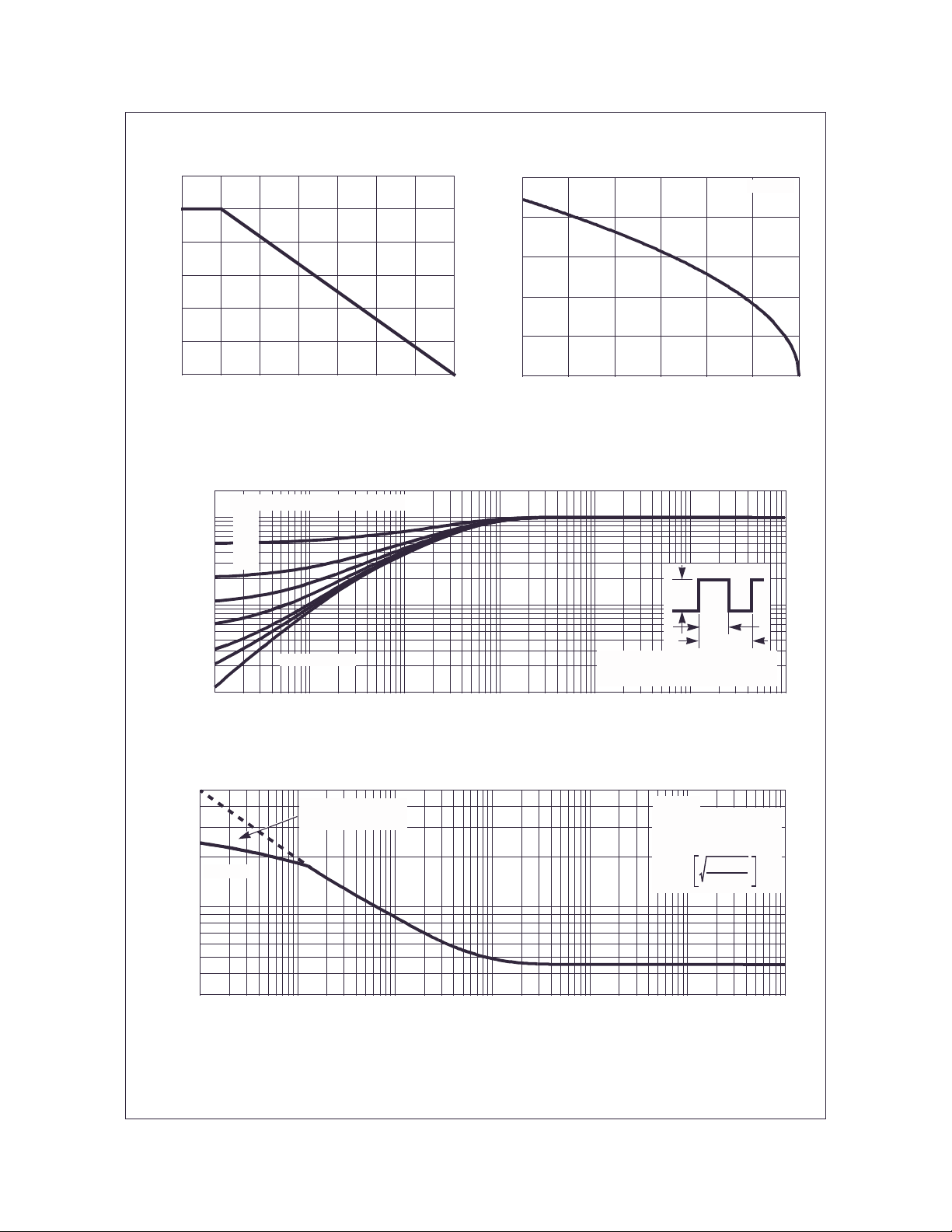
1.2
1.0
0.8
0.6
0.4
0.2
POWER DISSIPATION MULTIPLIER
0
0255075100 175
125
TC, CASE TEMPERATURE (oC)
Figure 1. Normalized Power Dissipation vs
Ambient Temperature
2
DUTY CYCLE - DESCENDING ORDER
0.5
1
0.2
0.1
0.05
0.02
0.01
150
50
V
= 10V
GS
40
30
20
, DRAIN CURRENT (A)
D
I
10
0
25 50 75 100 125 150 175
TC, CASE TEMPERATURE (oC)
Figure 2. Maximum Continuous Drain Curr ent vs
Case Temperature
, NORMALIZED
Z
, PEAK CURRENT (A)
I
θJC
DM
THERMAL IMPEDANCE
500
100
30
0.1
0.01
10
-5
10
VGS = 10V
-5
SINGLE PULSE
-4
10
-3
10
-2
10
NOTES:
DUTY FACTOR: D = t
PEAK TJ = PDM x Z
-1
10
t, RECTANGULAR PULSE DURATION (s)
Figure 3. Normalized Maximum Transient Thermal Impedance
TRANSCONDUCTANCE
MAY LIMIT CURRENT
IN THIS REGION
-4
10
-3
10
t, PULSE WIDTH (s)
-2
10
-1
10
TC = 25oC
FOR TEMPERATURES
ABOVE 25
CURRENT AS FOLLOWS:
I = I
P
DM
1/t2
x R
θJC
0
10
o
25
0
10
t
1
t
2
+ T
θJC
C
C DERATE PEAK
175 - T
C
150
1
10
1
10
Figure 4. Peak Current Capability
©2002 Fairchild Semiconductor Corporation FDD3672 Rev. A
Typical Characteristics T
= 25°C unless otherwise noted
C
FDD3672
300
If R = 0
tAV = (L)(IAS)/(1.3*RATED BV
If R ≠ 0
t
= (L/R)ln[(IAS*R)/(1.3*RATED BV
AV
100
10
, AVALANCHE CURRENT (A)
AS
I
STARTING TJ = 150oC
1
0.001 0.01 0.1 1
tAV, TIME IN AVALANCHE (ms)
- VDD)
DSS
- VDD) +1]
DSS
STARTING TJ = 25oC
NOTE: Refer to Fairchild Application Notes AN7514 and AN7515
Figure 5. Unclamped Inductive Switching
Capability
80
TC = 25oC
60
40
, DRAIN CURRENT (A)
20
D
I
0
0 0.5 1.0 1.5 2.0 2.5 3.0
VGS = 10V
PULSE DURATION = 80µs
DUTY CYCLE = 0.5% MAX
VGS = 5V
VDS, DRAIN TO SOURCE VOLTAGE (V)
VGS = 7V
VGS = 6V
80
PULSE DURATION = 80µs
DUTY CYCLE = 0.5% MAX
V
= 15V
DD
60
40
TJ = 25oC
20
, DRAIN CURRENT (A)
D
I
0
10
3.5 4.0 4.5 5.0 5.5 6.0 6.5
VGS, GATE TO SOURCE VOLTAGE (V)
TJ = 175oC
TJ = -55oC
Figure 6. Transfer Characteristics
40
PULSE DURATION = 80µs
DUTY CYCLE = 0.5% MAX
35
30
25
20
15
DRAIN TO SOURCE ON RESISTANCE (m Ω)
0 1020304050
VGS = 6V
VGS = 10V
I
, DRAIN CURRENT (A)
D
Figure 7. Saturation Characte risti cs Figure 8. Drain to Sou rce On Resistanc e vs Dr ain
Current
2.5
PULSE DURATION = 80µs
DUTY CYCLE = 0.5% MAX
2.0
1.5
ON RESISTANCE
1.0
NORMALIZED DRAIN TO SOURCE
0.5
-80 -40 0 40 80 120 160 200
TJ, JUNCTION TEMPERATURE (oC)
VGS = 10V, ID = 44A
Figure 9. Normalized Drain to Source On
Resistance vs Junction Temperature
©2002 Fairchild Semiconductor Corporation FDD3672 Rev. A
1.2
VGS = VDS, ID = 250µA
1.0
0.8
NORMALIZED GATE
0.6
THRESHOLD VOLTAGE
0.4
-80 -40 0 40 80 120 160 200
TJ, JUNCTION TEMPERATURE (oC)
Figure 10. Normalized Gat e Threshol d Voltage vs
Junction Temperatur e
 Loading...