

Fairchild Semiconductor FDD3570 Datasheet
FDD3570
80V N-Channel PowerTrench MOSFET
FDD3570
February 2000
PRELIMINARY
General Description
This N-Channel Logic level MOSFET has been
designed specifically to improve the overall effici ency of
DC/DC converters using either synchronous or
conventional switching PWM controllers.
Features
10 A, 80 V. R
•
R
Fast switching speed.
•
= 0.019 Ω @ VGS = 10 V
DS(ON)
= 0.022 Ω @ VGS = 6 V.
DS(ON)
This MOSFET features faster switching and lower gate
change than other MOSFETs with comparable R
specifications resulting in DC/DC power supply des igns
with higher overall efficiency.
DS(ON)
High performance trench technology for extremely
•
DS(ON)
.
low R
High power and current handling capability.
•
D
D
G
S
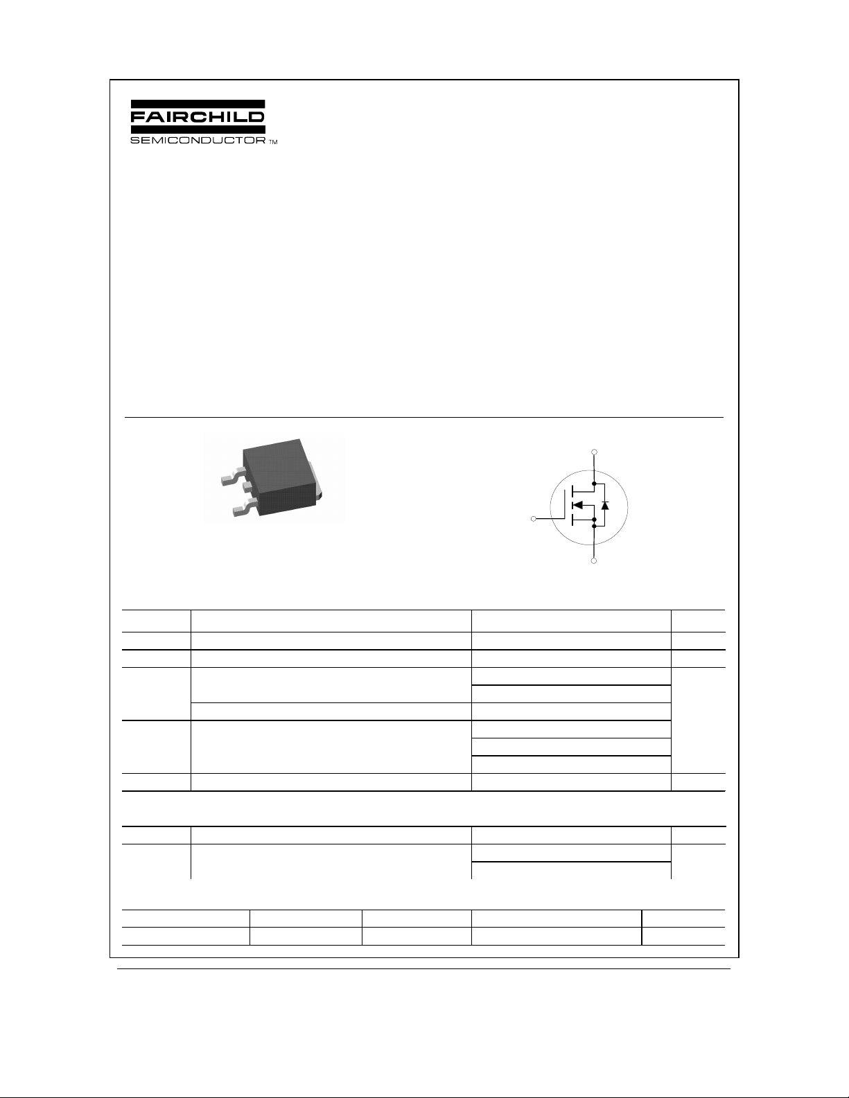
G
TO-252
S
Absolute Maximum Ratings
TA=25oC unless otherwise noted
Symbol Parameter Ratings Units
V
DSS
V
GSS
I
D
P
D
TJ, T
stg
Drain-Source Voltage 80 V
Gate-Source Voltage
Maximum Drain Current-Continuous
(Note 1)
(Note 1a)
20
±
43
10
Maximum Drain Current – Pulsed 110
Maximum Power Dissipation @TC = 25oC
TA = 25oC
TA = 25oC
(Note 1)
(Note 1a)
(Note 1b)
69
3.4
1.3
Operating and Storage Junction Temperature Range -55 to +150
W
°
V
A
C
Thermal Characteristics
R
JC
θ
R
JA
θ
Thermal Resistance, Junction-to- Case
Thermal Resistance, Junction-to- Ambient
(Note 1)
(Note 1a)
(Note 1b)
1.8
37
96
Package Marking and Ordering Information
Device Marking Device Reel Size Tape width Quantity
FDD3570 FDD3570 13’’ 16mm 2500
2000 Fairchild Semiconductor Corpor ation
C/W
°
C/W
°
C/W
°
FDD3570 Rev BW)
FDD3570
Electrical Characteristics
TA = 25°C unless otherwise noted16
Symbol Parameter Test Conditions Min Typ Max Units
Off Characteristics
BV
DSS
DSS
BV
∆
T
∆
J
I
DSS
I
GSSF
I
GSSR
On Characteristics
V
GS(th)
GS(th)
V
∆
T
∆
J
R
DS(on)
I
D(on)
g
FS
Drain–Source Breakdown Voltage
Breakdown Voltage Temperature
Coefficient
V
= 0 V, ID = 250 µA
GS
I
= 250 µA,Referenced to 25°C
D
Zero Gate Voltage Drain Current VDS = 64 V, VGS = 0 V 1
Gate–Body Leakage Current,
VGS = 20 V, VDS = 0 V 100 nA
80 V
78
mV/°C
µ
Forward
Gate–Body Leakage Current,
VGS = –20 V VDS = 0 V –100 nA
Reverse
(Note 2)
Gate Threshold Voltage
Gate Threshold Voltage
Temperature Coefficient
Static Drain–Source
On–Resistance
V
= VGS, ID = 250 µA
DS
= 250 µA,Referenced to 25°C
I
D
VGS = 10 V, ID = 10 A
= 10 V, ID = 10 A,TJ =125°C
V
GS
V
= 6 V, ID = 9 A
GS
22.44 V
-7
0.015
0.027
0.016
0.019
0.038
0.022
mV/°C
On–State Drain Current VGS = 10 V, VDS = 5 V 25 A
Forward Transconductance VDS = 5 V, ID = 14 A 40 S
A
Ω
Dynamic Characteristics
C
iss
C
oss
C
rss
Input Capacitance 2800 pF
Output Capacitance 230 pF
Reverse Transfer Capacitance
= 40 V, V
V
DS
f = 1.0 MHz
GS
= 0 V,
117 pF
Switching Characteristics
t
t
t
t
Q
Q
Q
d(on)
r
d(off)
f
g
gs
gd
Turn–On Delay Time 20 32 ns
Turn–On Rise Time 12 24 ns
Turn–Off Delay Time 60 95 ns
Turn–Off Fall Time
Total Gate Charge 54 76 nC
Gate–Source Charge 9.6 nC
Gate–Drain Charge
(Note 2)
V
= 40 V, ID = 1 A,
DD
= 10 V, R
V
GS
= 40V, ID = 9 A,
V
DS
= 10 V
V
GS
GEN
= 6
Ω
24 38 ns
14 nC
Drain–Source Diode Characteristics and Maximum Ratings
I
S
V
SD
Notes:
is the sum of the junction-to-case and case-to-ambient thermal resistance where the case thermal reference is defined as the solder mounting surface of
R
1.
JA
θ
the drain pins. R
Scale 1 : 1 on letter size paper
Pulse Test: Pulse Width < 300µs, Duty Cycle < 2.0%
2.
Maximum Continuous Drain–Source Diode Forward Current 2.8 A
Drain–Source Diode Forward
VGS = 0 V, IS = 2.8 A
(Note 2)
0.72 1.2 V
Voltage
is guaranteed by design while R
JC
θ
is determined by the user's board design.
CA
θ
a) R
= 40°/W when mounted on a
JA
θ
1in2 pad of 2 oz copper
b) R
= 96°/W when mounted on
JA
θ
a minimum pad.
FDD3570 Rev. A(W)
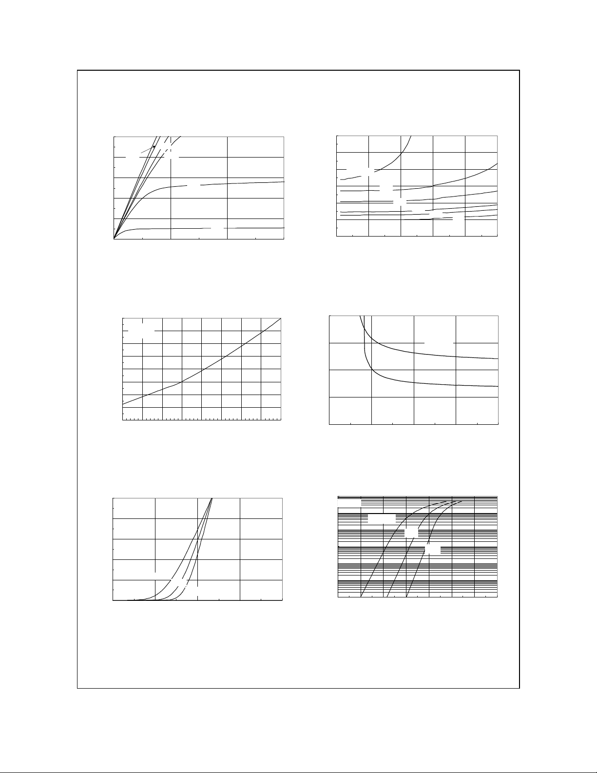
Typical Characteristics
V
FDD3570
50
VGS = 10V
6.0V
40
30
20
, DRAIN CURRENT (A)
D
I
10
0
0123
5.0V
4.5V
4.0
3.5V
V
, DRAIN-SOURCE VOLTAGE (V)
DS
2
1.8
1.6
VGS = 4.0V
1.4
, NORMALIZED
1.2
DS(ON)
R
1
DRAIN-SOURCE ON-RESISTANCE
0.8
0 1020304050
4.5V
5.0V
6.0V
, DRAIN CURRENT (A)
I
D
7.0V
Figure 1. On-Region Characteristics. Figure 2. On-Resistance Variation with
Drain Current and Gate Voltage.
2
ID = 9A
1.8
= 10V
V
GS
1.6
1.4
1.2
, NORMALIZED
1
DS(ON)
R
0.8
0.6
DRAIN-SOURCE ON-RESISTANCE
0.4
-50 -25 0 25 50 75 100 125 150
, JUNCTION TEMPERATURE (oC)
T
J
0.04
0.03
0.02
, ON-RESISTANCE (OHM)
0.01
DS(ON)
R
0
246810
V
, GATE TO SOURCE VOLTAGE (V)
GS
TA = 125oC
TA = 25oC
10V
ID = 10 A
Figure 3. On-Resistance Variation with
Temperature.
50
VDS = 5V
40
30
20
, DRAIN CURRENT (A)
D
I
10
0
23456
125oC
25oC
TA = -55oC
V
, GATE TO SOURCE VOLTAGE (V)
GS
Figure 4. On-Resistance Variation with
Gate-to-Source Voltage.
100
VGS = 0V
10
1
0.1
0.01
0.001
, REVERSE DRAIN CURRENT (A)
S
I
0.0001
0 0.2 0.4 0.6 0.8 1 1.2 1.4
TA = 125oC
25oC
-55oC
, BODY DIODE FORWARD VOLTAGE (V)
V
SD
Figure 5. Transfer Characteristics. Figure 6. Body Diode Forward Voltage Variation
with Source Current and Temperature.
FDD3570 Rev. A(W)
 Loading...