

Fairchild Semiconductor FDD10AN06A0 Datasheet
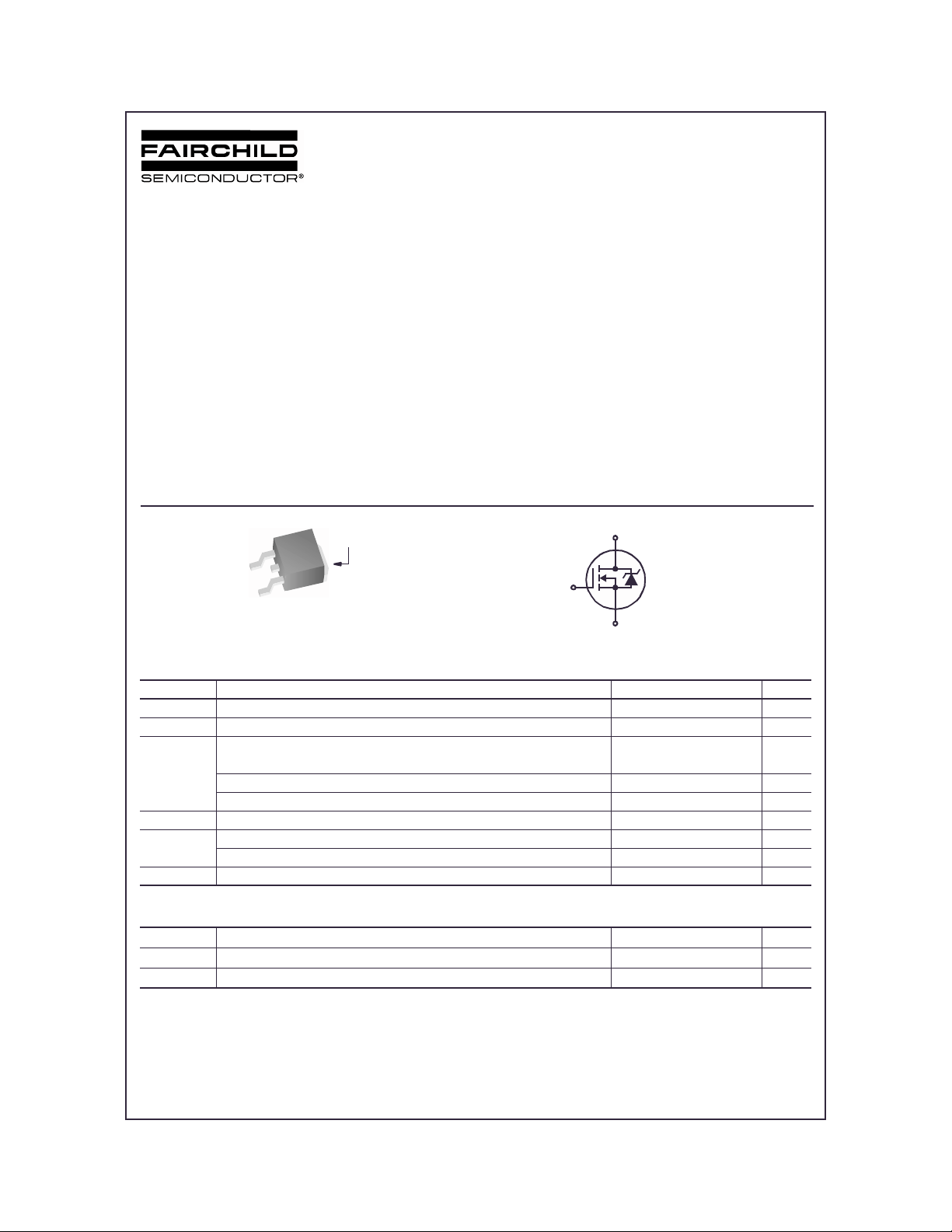
FDD10AN06A0
N-Channel PowerTrench® MOSFET
60V, 50A, 10.5mΩ
FDD10AN06A0
August 2002
Features
•r
•Q
• Low Miller Charge
• Low Qrr Body Diode
• UIS Capability (Single Pulse and Repetitive Pulse)
• Qualified to AEC Q101
Formerly developmental type 82560
MOSFET Maximum Ratings T
= 9.4mΩ (Typ.), V
DS(ON)
(tot) = 28nC (Typ.), V
g
GATE
SOURCE
TO-252AA
FDD SERIES
= 10V, ID = 50A
GS
= 10V
GS
(FLANGE)
DRAIN
= 25°C unless otherwise not ed
C
Applications
• Motor / Body Load Control
• ABS Systems
• Powertrain Management
• Injection Syste m s
• DC-DC converter s and Off-line UPS
• Distributed P ower Arc hitectures and VRMs
• Primary Switch for 12V and 24V systems
D
G
S
Symbol Parameter Ratings Units
V
DSS
V
GS
Drain to Sou r c e Voltage 60 V
Gate to Source Voltage ±20 V
Drain Curr e nt
I
D
Continuous (T
Continuous (T
< 115oC, VGS = 10V)
C
= 25oC, VGS = 10V, with R
amb
= 52oC/W) 11 A
θJA
50 A
Pulsed Figure 4 A
E
AS
P
D
, T
T
J
STG
Single Pulse Avalanche Energy (Note 1) 429 mJ
Power dissipation 135 W
Derate above 25
o
C0.9W/
Operating and Storage Temperature -55 to 175
o
C
o
C
Thermal Characteristics
R
θJC
R
θJA
R
θJA
This product has been designed to meet the extreme test conditions an d environment dem anded by the au tomotive industry. For a
All Fairchild Semiconductor products are manufactu red, assembled and tested under ISO9000 and QS9000 quality systems
©2002 Fairchild Semiconductor Corporation
Thermal Resistance Junction to Case TO-252 1.11
Thermal Resistance Junction to Ambient TO-252 100
Thermal Resistance Junction to Ambient TO-252, 1 in2 copper pad area 52
copy of the requirements, see AEC Q101 at: http://www.aecouncil.com/
Reliability data can be fou nd a t: http://ww w.f airc hilds e m i.co m /pr oduc ts/dis c rete/reliab ility/ind ex.html.
certification.
FDD10AN06A0 Rev. A
o
C/W
o
C/W
o
C/W
Package Marking and Ordering Information
Device Marking Device Package Reel Size Tape Width Quantity
FDD10AN 06A0 FDD10AN06A0 TO-252AA 330m m 16mm 2500 units
FDD10AN06A0
Electrical Characteristics
TC = 25°C unless otherwise noted
Symbol Parameter Test Con ditions Min Typ Max Units
Off Characteristics
B
I
DSS
I
GSS
VDSS
Drain to Sou r c e Br ea k down Voltage ID = 250µA, VGS = 0V 60 - - V
V
= 50V - - 1
Zero Gate Voltage Drain Current
DS
= 0V TC = 150oC- -250
V
GS
Gate to Source Leakage Current VGS = ±20V - - ±100 nA
On Characteristics
V
GS(TH)
r
DS(ON)
Gate to Source Threshold Voltage VGS = VDS, ID = 250µA2-4V
I
= 50A, VGS = 10V - 0.0094 0.0105
D
I
= 25A, VGS = 6V - 0.015 0.027
Drain to S ou r c e On Re si st ance
D
I
= 50A, VGS = 10V,
D
T
= 175oC
J
- 0.020 0.023
Dynamic Characteristics
C
C
C
Q
Q
Q
Q
Q
ISS
OSS
RSS
g(TOT)
g(TH)
gs
gs2
gd
Input Capacitance
Output Capacitance - 340 - pF
Reverse Transfer Capacitance - 110 - pF
= 25V, VGS = 0V,
V
DS
f = 1MHz
Total Gate Charge at 10V VGS = 0V to 10V
Threshold Gate Charge VGS = 0V to 2V - 3.5 4.6 nC
Gate to Source Gate Charg e - 9.8 - nC
Gate Charge Threshold to Plateau - 6.4 - nC
V
DD
I
= 50A
D
I
= 1.0m A
g
= 30V
Gate to Drain “Miller” Charge - 7.8 - nC
- 1840 - pF
28 37 nC
µA
Ω
Switching Characteristics
t
ON
t
d(ON)
t
r
t
d(OFF)
t
f
t
OFF
Turn-On Time
Turn-On Delay Time - 8 - ns
Rise Time - 79 - ns
Turn-Off D elay Time - 32 - ns
Fall Time - 32 - ns
Turn-Off Time - - 97 ns
(VGS = 10V)
= 30V, ID = 50A
V
DD
V
= 10V, RGS = 10Ω
GS
--131ns
Drain-Source Diode Characteristics
I
= 50A - - 1.2 5 V
V
SD
t
rr
Q
RR
Notes:
1: Starting T
©2002 Fairchild Semiconductor Corporation FDD10AN06A0 Rev. A
Source to Drain Diode V oltage
Reverse Recovery Time ISD = 50A, dISD/dt = 100A/µs- -27ns
Reverse Recovered Charge ISD = 50A, dISD/dt = 100A/µs- -23nC
= 25°C, L = 8.58mH, IAS = 10A.
J
SD
= 25A - - 1.0 V
I
SD
FDD10AN06A0
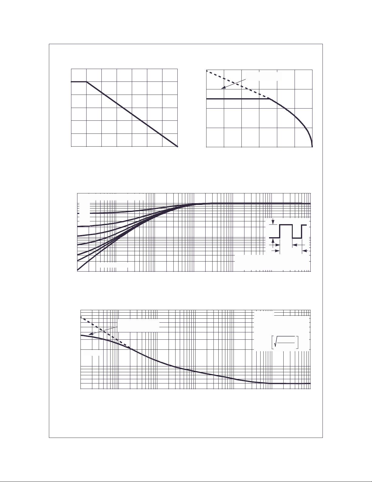
Typical Characteristics T
= 25°C unless otherwise noted
C
1.2
1.0
0.8
0.6
0.4
0.2
POWER DISSIPATION MULTIPLIER
0
0255075100 175
125
TC, CASE TEMPERATURE (oC)
Figure 1. Normalized Power Dissipation vs
Ambient Temperature
2
DUTY CYCLE - DESCENDING ORDER
0.5
1
0.2
0.1
0.05
0.02
0.01
0.1
, NORMALIZED
θJC
Z
THERMAL IMPEDANCE
0.01
-5
10
SINGLE PULSE
-4
10
10
80
60
40
, DRAIN CURRENT (A)
D
I
20
150
0
25 50 75 100 125 150 175
Figure 2. Maximum Continuous Drain Curr ent vs
-3
t, RECTANGULAR PULSE DURATION (s)
-2
10
CURRENT LIMITED
BY PACKAGE
TC, CASE TEMPERATURE (oC)
Case Temperature
P
DM
NOTES:
DUTY FACTOR: D = t
PEAK TJ = PDM x Z
-1
10
θJC
10
1/t2
x R
0
θJC
t
1
+ T
t
2
C
1
10
Figure 3. Normalized Maximum Transient Thermal Impedance
1000
TRANSCONDUCTANCE
MAY LIMIT CURRENT
IN THIS REGION
VGS = 10V
, PEAK CURRENT (A)
100
DM
I
40
-5
10
-4
10
-3
10
-2
10
-1
10
t, PUL SE WIDTH (s)
TC = 25oC
FOR TEMPERATURES
o
ABOVE 25
C DERATE PEAK
CURRENT AS FOLLOWS:
175 - T
I = I
25
10
C
150
0
1
10
Figure 4. Peak Current Capability
©2002 Fairchild Semiconductor Corporation FDD10AN06A0 Rev. A
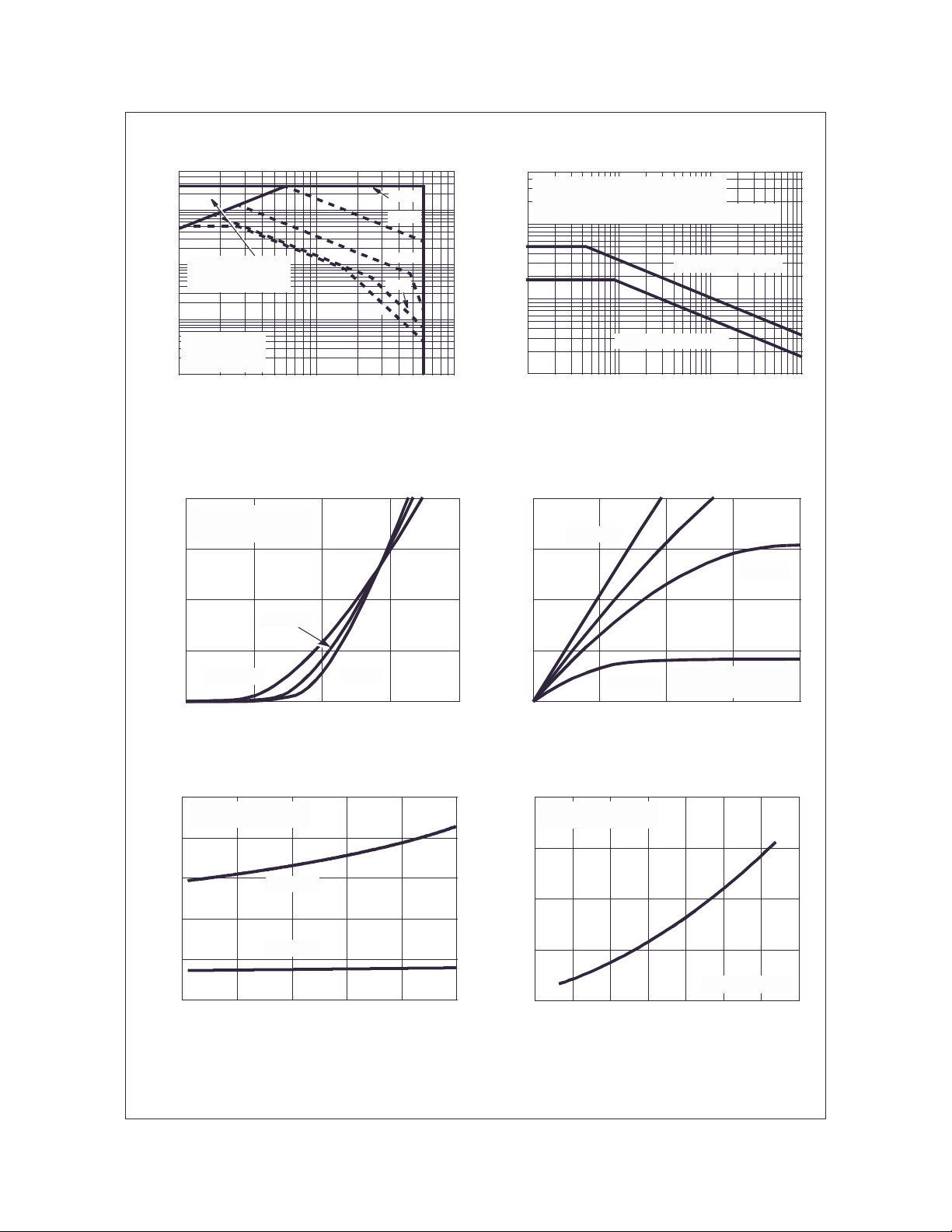
Typical Characteristics T
= 25°C unless otherwise noted
C
FDD10AN06A0
500
100
OPERATIO N IN THIS
10
, DRAIN CURRENT (A)
D
I
0.1
AREA MAY BE
LIMITED BY r
1
SINGLE PULSE
TJ = MAX RATED
= 25oC
T
C
110100
DS(ON)
V
, DRAIN TO SOURCE VOLTAGE (V)
DS
10µs
100µs
1ms
10ms
DC
Figure 5. Forward Bias Safe Operating Area
500
100
10
, AVALANCHE CURRENT (A)
AS
I
1
0.01
NOTE: Refer to Fairchild Application Notes AN7514 and AN7515
Figure 6. Unclamped Inductive Switching
100
PULSE DURATION = 80µs
DUTY CYCLE = 0.5% MAX
V
= 15V
DD
75
50
TJ = 25oC
, DRAIN CURRENT (A)
D
I
25
TJ = 175oC
0
34567
VGS, GATE TO SOURCE VOLTAGE (V)
TJ = -55oC
100
75
50
, DRAIN CURRENT (A)
D
I
25
0
0 0.5 1.0 1.5 2.0
If R = 0
tAV = (L)(IAS)/(1.3*RATED BV
If R ≠ 0
t
= (L/R)ln[(IAS*R)/(1.3*RATED BV
AV
ST ARTING TJ = 150oC
0.1 1 10
tAV, TIME IN AVALANCHE (ms)
Capability
VGS = 10V
TC = 25oC
VDS, DRAIN TO SOURCE VOLTAGE (V)
- VDD)
DSS
- VDD) +1]
DSS
STARTING TJ = 25oC
= 7V
V
GS
VGS = 6V
V
PULSE DURATION = 80µs
DUTY CYCLE = 0.5% MAX
= 5V
GS
Figure 7. Transfer Characteristics Figure 8. Saturation Characteristics
18
PULSE DURATION = 80µs
DUTY CYCLE = 0.5% MAX
16
14
12
10
DRAIN TO SOURCE ON RESISTANCE(mΩ)
8
0 1020304050
VGS = 6V
VGS = 10V
I
, DRAIN CURRENT (A)
D
Figure 9. Drain to So urce On Resistanc e v s Drai n
Current
©2002 Fairchild Semiconductor Corporation FDD10AN06A0 Rev. A
2.5
PULSE DURATION = 80µs
DUTY CYCLE = 0.5% MAX
2.0
1.5
ON RESISTANCE
1.0
NORMALIZED DRAIN TO SOURCE
0.5
-80 -40 0 40 80 120 160 200
TJ, JUNCTION TEMPERATURE (oC)
VGS = 10V, ID = 50A
Figure 10. Normalized Drain to Source On
Resistance vs Junction Temperature
 Loading...