Fairchild Semiconductor FDC6901L Datasheet

FDC6901L
Integrated Load Switch
General Description
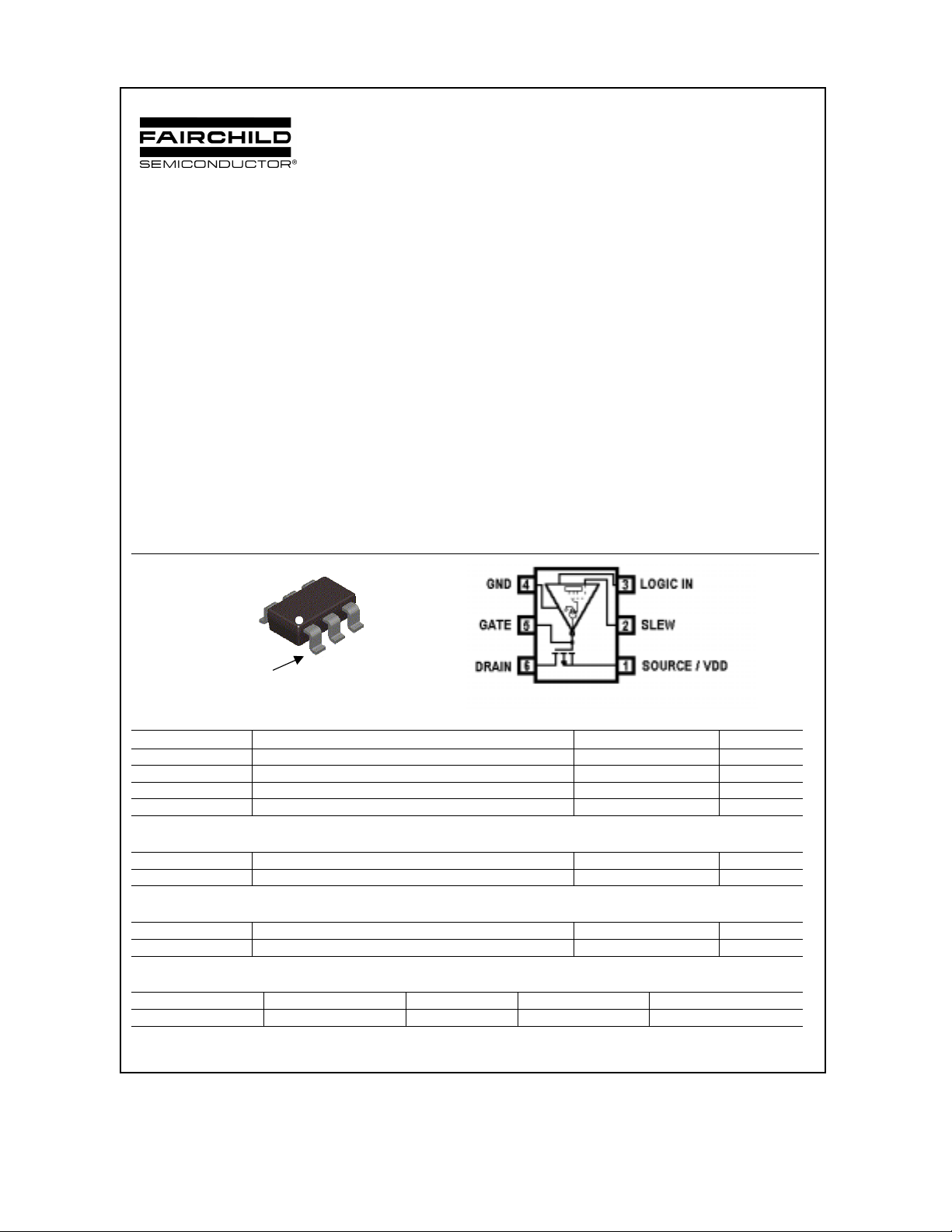
This device is particularly suited for compact power
management. In portabl e electronic equipm ent where 2.5V
to 6V input capability is needed. This load switch integrates
a Slew Rate Control Driver that drives a P-Channel Power
MOSFET in one tiny SuperSOT-6 package. The
integrated slew rate cont rol driver is specifically designed
to control the turn on of the P-Channel MOSFET in order to
limit the inrush current in battery switching applications with
high capacitance loads. For turn-off, the IC pulls the
MOSFET gate up quickly.
Applications
• Load switch
• Power management
D2
S1
D1
May 2002
Features
• Three programmable slew rates
• Reduces inrush current
• Minimizes EMI
• Normal turn-off speed
• Low-power CMOS operates over wide voltage range
• High performance trench te chnology for extremely
low R
DS(ON)
FDC6901L
G2
G1
S2
=25oC unless otherwise noted
A
SuperSOT -6
TM
Pin 1
SuperSOT™-6
Absolute Maximum Ratings T
Symbol Parameter Ratings Units
VDD Supply Voltage –0.5 to 10 V
VIN DC Input Voltage (Logic Inputs) –0.7 to 6 V
PD Power Dissipation
T
Storage Junction Temperat ure Range –55 to +150 °C
STG
Recommended Operating Range
VDD Supply Voltage –0.5 to 10 V
TJ Operating Junction Temperat ure –55 to +150 °C
Thermal Characteristics
R
θJA
R
θJC
Thermal Resistance, Junction to Ambient 180 °C/W
Thermal Resistance, Junction to Case 60 °C/W
Package Marking and Ordering Information
Device Marking Device Reel Size Tape Width Quantity
.901 FDC6901L 7” 8mm 3000 units
2002 Fairchild Semiconductor Corporation
FDC6901L Rev C (W)

µ
µ
Electrical Characteristics T
=25oC unless otherwise noted
A
FDC6901L
Symbol Parameter Test Conditions Min Typ Max Units
Logic Levels
VIH Logi c HIGH Input Voltage VDD = 2.7 V to 6.0 V
VIL Logic LOW Input Voltage VDD = 2.7 V to 6.0 V
75%*
V
DD
25%*
V
V
DD
V
OFF Characteristics – Slew Rate Control Driver
BVDG Supply Input Breakdown Voltage I
BV
Sl ew Input Breakdown Voltage I
SLEW
BVIN Logic Input Breakdown Voltage I
IRDG Supply Input Leakage Current V
IR
Slew Input Leakage Current V
SLEW
IRIN Logic Input Leakage Current V
= 10 µA, V
DG
= 10 µA, V
SLEW
= 10 µA, V
IN
= 8 V, V
DG
= 8 V, V
SLEW
= 8 V, V
IN
= 0 V, V
IN
= 0 V 9 V
IN
= 0 V 9 V
SLEW
= 0 V, V
IN
= 0 V 100 nA
IN
= 0 V 100 nA
SLEW
= 0 V 9 V
SLEW
= 0 V 100 nA
SLEW
OFF Characteristics – Slew Rate Control Driver + P-Channel MOSFET
BVIO IO Breakdown Voltage
I
= –250 µA
D
IRIO IO Leakage Current VR = 16 V 100 nA
9 V
ON Characteristics – Slew Rate Control Driver
IG Output/Gate Current VIN = 6V
= 2V
V
GATE
Slew Pin = OPEN
= GROUND
= V
DD
90
1
10
µA
µA
nA
ON Characteristics – P-Channel MOSFET
V
Gate Threshold Voltage
GS(th)
R
Stat i c Drain-Source On
DS(ON)
Resistance
V
= VGS , ID = –250 µA
DS
V
= –4.5 V, ID = –1.5 A
GS
= –2.5 V, ID = –1.2 A
V
GS
–0.6 –1.0 –1.5 V
120
170
145
210
mΩ
mΩ
ON Characteristics – Slew Rate Control Driver + P-Channel MOSFET
V
Dropout Voltage VDD = 6V, VIN = 2.5V to 6V, IL = 1.5 A
DROP
= 6V, VIN = 2.5V to 6V, IL = 1.2 A
V
DD
RON Load switch On Resistance VDD = 6V, VIN = 2.5V to 6V, IL = 1.5 A
= 6V, VIN = 2.5V to 6V, IL = 1.2 A
V
DD
I
Load Current
LOAD
V
= 2.5 V, VDS = 6 V
GS
160
130
105
110
3 A
300
300
180
210
mV
mV
mΩ
mΩ
P-Channel MOSFET Switching Times
Vsupply = 5.5V, VDD = 5.5V, Logic IN = 5.5V, I
Output Turn-On Delay Ti me S l ew Pin = OP E N
t
don
t
Output Rise Time Slew Pin = OPEN
rise
dv/dt Output Slew Rate Slew Pin = OPEN
= 1.5A
LOAD
= GROUND
= V
DD
= GROUND
= V
DD
= GROUND
= V
DD
6.20
42
115
6.75
124
162
600
41
24
µs
µs
s
µs
µs
s
V/ms
V/ms
V/ms
FDC6901L Rev C (W)
 Loading...