

Fairchild Semiconductor FDC642P Datasheet
FDC642P
P-Channel 2.5V Specified PowerTrenchTM MOSFET
FDC642P
July 1999
General Description
This P-Channel 2.5V specified MOSFET is produced
using Fairchild's advanced PowerTrench process that
has been especially tailored to minimize on-state
resistance and yet maintain low gate charge for
superior switching performance.
These devices have been designed to offer exceptional
power dissipation in a very small footprint for
applications where the larger packages are impractical.
Applications
Load switch
Features
-4 A, -20 V. R
R
DS(ON)
DS(ON)
= 0.065 Ω @ V
= 0.100 Ω @ V
= -4.5 V
GS
= -2.5 V
GS
Fast switching speed.
Low gate charge (7.2nC typical).
High performance trench technology for extremely
low R
SuperSOT
than standard SO-8); low profile (1mm thick).
.
DS(ON)
TM
-6 package: small footprint (72% smaller
Battery protection
Power management
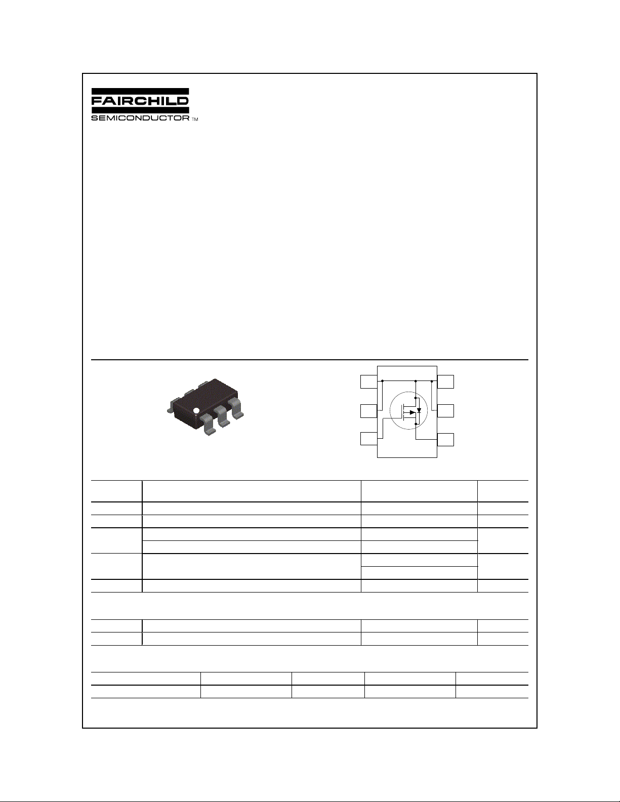
S
D
1
6
D
5
4
G
SuperSOT -6
TM
D
D
Absolute Maximum Ratings T
= 25°C unless otherwise noted
A
2
3
3
Symbol Parameter Ratings Units
V
DSS
V
GSS
I
D
P
D
TJ, T
stg
Drain-Source Voltage -20 V
Gate-Source Voltage
Drain Current - Continuous (Note 1) -4 A
Drain Current - Pulsed (Note 1a) -20
Power Dissipation for Single Operat i on (Note 1a) 1.6 W
(Note 1b)
Operating and Storage Junction Temperature Range -55 to +150
±8
0.8
°C
V
Thermal Characteristics
R
JA
θ
R
JC
θ
Thermal Resistance, Junction-to-Amb i ent (Note 1a) 78
Thermal Resistance, Junction-to-Case (Note 1) 30
Package Outlines and Ordering Information
Device Marking Device Reel Size Tape Width Quantity
.642 FDC642P 7’’ 8mm 3000 units
1999 Fairchild Semiconductor Corporation
°C/W
°C/W
FDC642P, Rev. B
FDC642P
Electrical Characteristics T
= 25°C unless otherwise noted
A
Symbol Parameter Test Conditions Min Typ Max Units
Off Characteristics
BV
DSS
∆BVDSS
∆T
J
I
DSS
I
GSSF
I
GSSR
Drain-Source Breakdown Voltage
Breakdown Voltage Temperature
Coefficient
= 0 V, ID = -250 µA
V
GS
= -250 µA, Referenced to 25°C
I
D
Zero Gate Voltage Drain Current VDS = -16 V, VGS = 0 V -1
Gate-Body Leakage Current, Forward VGS = 8 V, VDS = 0 V 100 nA
Gate-Body Leakage Current, Reverse VGS = -8 V, VDS = 0 V -100 nA
-20 V
-16
mV/°C
µA
On Characteristics (Note 2)
V
GS(th)
∆VGS(th)
∆T
J
R
DS(on)
I
D(on)
g
FS
Gate Threshold Voltage
Gate Threshold Voltage
Temperature Coefficient
Static Drain-Source
On-Resistance
= VGS, ID = -250 µA
V
DS
= -250 µA, Referenced to 25°C
I
D
VGS = -4.5 V, ID = -4 A
V
= -4.5 V, ID = -4 A, TJ=125°C
GS
V
= -2.5 V, ID = -3.2 A
GS
On-State Drain Current VGS = -4.5 V, VDS = -5 V -10 A
Forward Transconductance VDS = -5 V, ID = -4 A 9 S
-0.4 -0.7 -1.5 V
2.5
0.054
0.076
0.077
mV/°C
0.065
0.105
0.100
Ω
Dynamic Characteristics
C
iss
C
oss
C
rss
Input Capacitance 640 pF
Output Capacitance 180 pF
Reverse Transfer Capacitance
V
= -10 V, VGS = 0 V
DS
f = 1.0 MHz
90 pF
Switching Characteristics (Note 2)
t
d(on)
t
r
t
d(off)
t
f
Q
Q
Q
g
gs
gd
Turn-On Delay Time 11 20 ns
Turn-On Rise Time 19 30 ns
= -10 V, ID = -1 A
V
DD
V
= -4.5 V, R
GS
GEN
= 6 Ω
Turn-Off Delay Time 26 42 ns
Turn-Off Fall Time
Total Gate Charge 7.2 10 nC
Gate-Source Charge 1.7 nC
V
= -10 V, ID = -4 A
DS
= -4.5 V,
V
GS
Gate-Drain Charge
Drain-Source Diode Characteristics and Maximum Ratings
I
S
V
SD
Notes:
1. R
θJA
of the drain pins. R
2. Pulse Test: Pulse Width ≤ 300 µs, Duty Cycle ≤ 2.0%
Maximum Continuous Drain-Source Diode Forward Current -1.3 A
Drain-Source Diode Forward Voltage VGS = 0 V, IS = -1.3 A (Note 2) -0.75 -1.2 V
is the sum of the junction-to-case and case-to-ambient thermal resistance where the case thermal reference is defined as the solder mounting surface
a) 78° C/W when mounted on a 1.0 in2 pad of 2 oz. copper.
b) 156° C/W when mounted on a minimum pad of 2 oz.copper.
is guaranteed by design while R
θJC
is determined by the user's board design.
θCA
35 55 ns
1.6 nC
FDC642P, Rev. B
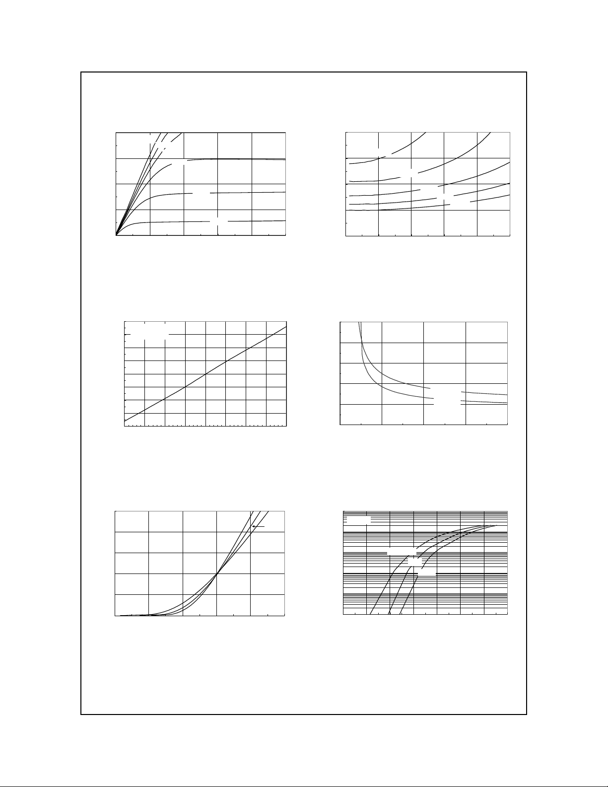
Typical Characteristics
FDC642P
20
VGS = -4.5V
-3.5V
15
10
5
, DRAIN-SOURCE CURRENT (A)
D
-I
0
012345
-3.0V
-2.5V
-2.0V
-1.5V
-V
, DRAIN-SOURCE VOLTAGE (V)
DS
Figure 1. On-Region Characteristics.
1.5
ID = - 4A
V
1.4
1.3
1.2
1.1
, NORMALIZED
DS(ON)
0.9
R
0.8
DRAIN-SOURCE ON- RESISTANCE
0.7
= - 4.5V
GS
1
-50 -25 0 25 50 75 100 125 150
T
, JUNCTION TEMP E RATURE (oC)
J
1.6
VGS = -2.5V
1.4
-3.0V
1.2
, NORMALIZED
DS(ON)
R
1
DRAIN-SOURCE ON-RESISTANCE
0.8
048121620
-3.5V
-4.0V
- I
, DRAIN CURRENT (A)
D
-4.5V
Figure 2. On-Resistance Variation
with Drain Current and Gate Voltage.
0.25
ID = -2A
0.2
0.15
0.1
, ON-RESISTANCE (OHM)
0.05
DS(ON)
R
0
12345
-V
, GATE TO SOURCE VOL TAGE (V)
GS
TA = 125oC
TA = 25oC
Figure 3. On-Resistance Variation
with Temperature.
10
VDS = -5V
8
6
4
, DRAIN CURRENT (A)
D
-I
2
0
0.4 0.8 1.2 1.6 2 2.4
-V
, GATE TO SOURCE VOLTAGE (V)
GS
TA = -55oC
125oC
25oC
Figure 4. On-Resistance Variation
with Gate-to-Source Voltage.
100
VGS = 0V
10
1
0.1
0.01
, REVERSE DRAIN CURRENT (A)
S
-I
0.001
0 0.2 0.4 0.6 0.8 1 1.2 1.4
T = 125oC
25oC
-55oC
, BODY DIODE FORWARD VOLTAGE (V)
-V
SD
Figure 5. Transfer Characteristics. Figure 6. Body Diode Forward Voltage
Variation with Source Current
and Temperature.
FDC642P, Rev. B
 Loading...