

Fairchild Semiconductor FDC6392S Datasheet
April 2002
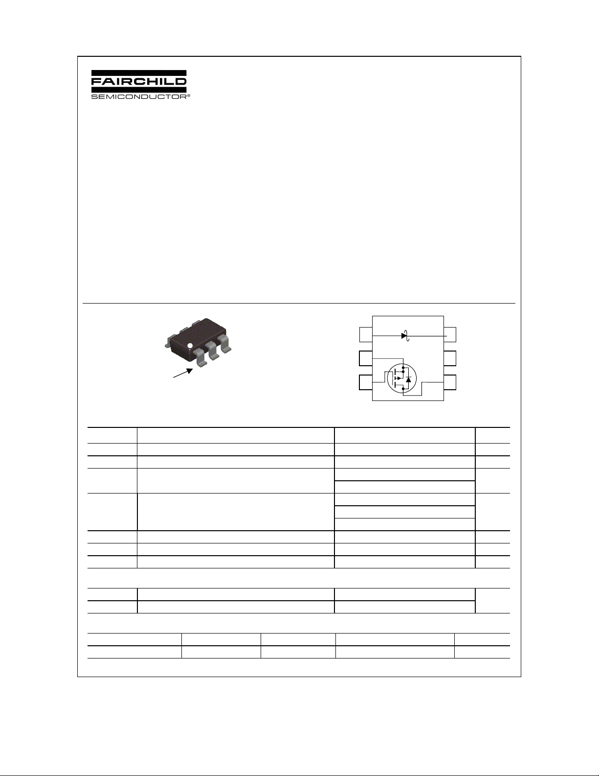
FDC6392S
20V Integrated P-Channel PowerTrench
MOSFET and Schottky Diode
FDC6392S
General Description
The FDC6392S combines the exceptional performance
of Fairchild's PowerTrench MOSFET technology with a
very low forward voltage drop Schottky barrier rectifier
in an SSOT-6 package.
This device is designed specifically as a single package
solution for DC to DC converters. It features a fast
switching, low gate charge MOSFET with very low onstate resistance. The independently connected
Schottky diode allows its use in a variety of DC/DC
converter topologies.
D2
S1
D1
G2
G1
S2
o
=25
C unless otherwise noted
A
SuperSOT -6
TM
Pin 1
SuperSOT™-6
Absolute Maximum Ratings T
Features
MOSFET:
• –2.2 A, –20V. R
R
• Low Gate Charge (3.7nC typ)
• Compact industry standard SuperSOT
Schottky:
• VF < 0.45 V @ 1 A
1
2
3
= 150 mΩ @ VGS = –4.5V
DS(ON)
= 200 mΩ @ VGS = –2.5V
DS(ON)
6
5
4
-6 package
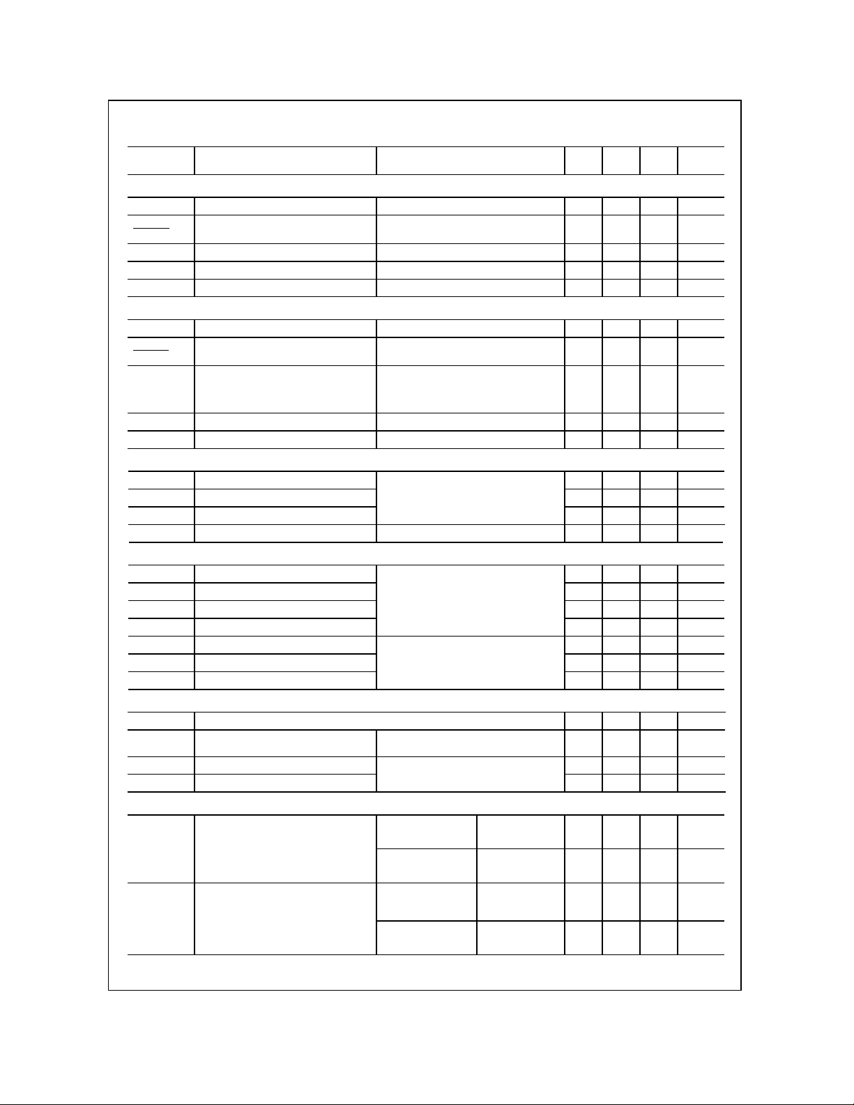
Symbol Parameter Ratings Units
V
MOSFET Drain-Source Voltage –20 V
DSS
V
MOSFET Gate-Source Voltage
GSS
±12
ID Drain Current – Continuous (Note 1a) –2.2 A
– Pulsed –6
PD
TJ, T
STG
V
Schottky Repetitive Peak Reverse Voltage 20 V
RRM
Power Dissipation for Single Operation (Note 1a) 0.96
(Note 1b)
(Note 1c)
0.9
0.7
Operating and Storage Junction Temperature Range –55 to +150
IO Schottky Average Forward Current (Note 1a) 1 A
V
W
°C
Thermal Characteristics
R
θJA
R
θJC
Thermal Resistance, Junction-to-Ambient
Thermal Resistance, Junction-to-Case
(Note 1a) 130
(Note 1) 60
Package Marking and Ordering Information
Device Marking Device Reel Size Tape width Quantity
2002 Fairchild Sem iconductor Corporation
.392 FDC6392S 7’’ 8mm 3000 units
°C/W
FDC6392S Rev C(W )
FDC6392S
Electrical Characteristics T
= 25°C unless otherwise noted
A
Symbol Parameter Test Conditions Min Typ Max Units
Off Characteristics
BV
Drain–Source Breakdown Voltage
DSS
∆BVDSS
∆T
J
I
Zero Gate Voltage Drain Current VDS = –16 V, VGS = 0 V –1
DSS
I
Gate–Body Leakage, Forward VGS = 12 V, VDS = 0 V 100 nA
GSSF
I
Gate–Body Leakage, Reverse VGS = –12 V, VDS = 0 V –100 nA
GSSR
Breakdown Voltage Temperature
Coefficient
= 0 V, ID = –250 µA
V
GS
I
= –250 µA, Referenced to 25°C
D
–20 V
–16
mV/°C
µA
On Characteristics (Note 2)
V
Gate Threshold Voltage
GS(th)
∆VGS(th)
∆TJ
R
DS(on)
Gate Threshold Voltage
Temperature Coefficient
Static Drain–Source
On–Resistance
I
On–State Drain Current VGS = –4.5 V, VDS = –5 V –6 A
D(on)
= VGS, ID = –250 µA
V
DS
= –250 µA, Referenced to 25°C
I
D
VGS = –4.5 V, ID = –2.2 A
= –2.5 V, ID = –1.8 A
V
GS
=–4.5 V, ID =–2.2 A, TJ=125°C
V
GS
gFS Forward Transconductance VDS = –5 V, ID = –2.2 A 6 S
–0.6 –1.0 –1.5 V
3
101
152
132
150
200
211
mV/°C
mΩ
Dynamic Characteristics
C
Input Capacitance 369 pF
iss
C
Output Capacitance 80 pF
oss
C
Reverse Transfer Capacitance
rss
RG Gate Resistance VGS = –15 mV, f = 1.0 MHz 7.6
= –10 V, V
V
DS
f = 1.0 MHz
= 0 V,
GS
39 pF
Ω
Switching Characteristics (Note 2)
V
t
Turn–On Delay Time 8 16 ns
d(on)
tr Turn–On Rise Time 11 20 ns
t
Turn–Off Delay Time 13 23 ns
d(off)
tf Turn–Off Fall Time
Qg Total Gate Charge 3.7 5.2 nC
Qgs Gate–Source Charge 1 nC
Qgd Gate–Drain Charge
= –10 V, ID = –1 A,
DD
V
= –4.5 V, R
GS
V
= –10 V, ID = –2.2 A,
DS
= –4.5 V
V
GS
GEN
= 6 Ω
4 8 ns
1 nC
Drain–Source Diode Characteristics and Maximum Ratings
IS Maximum Continuous Drain–Source Diode Forward Current –0.8 A
VSD Drain–Source Diode Forward
Voltage
trr Diode Reverse Recovery Time 5.4 nS
Qrr Diode Reverse Recovery Charge
V
= 0 V, IS = –0.8 A(Note 2) –0.8 –1.2 V
GS
I
= –2.2 A,
F
= 100 A/µs
d
iF/dt
1.2 nC
Schottky Diode Characteristics
IR Reverse Leakage VR = 20 V
V
= 10V
R
VF Forward Voltage IF = 500mA
I
= 1 A
F
= 25°C
T
J
= 100°C
T
J
= 25°C
T
J
= 100°C
T
J
= 25°C
T
J
= 100°C
T
J
= 25°C
T
J
= 100°C
T
J
148 400
µA
14 20 mA
55 200
µA
5.2 10 mA
0.34 0.4 V
0.26 0.35
0.40 0.45 V
0.35 0.42
FDC6392S Rev C(W )
 Loading...