

Fairchild Semiconductor FDC6331L Datasheet
August 2001
3
2
145
6
Vout,C1
R2Vin,R
1
R1,C1
SeeApplicationCircuit
T
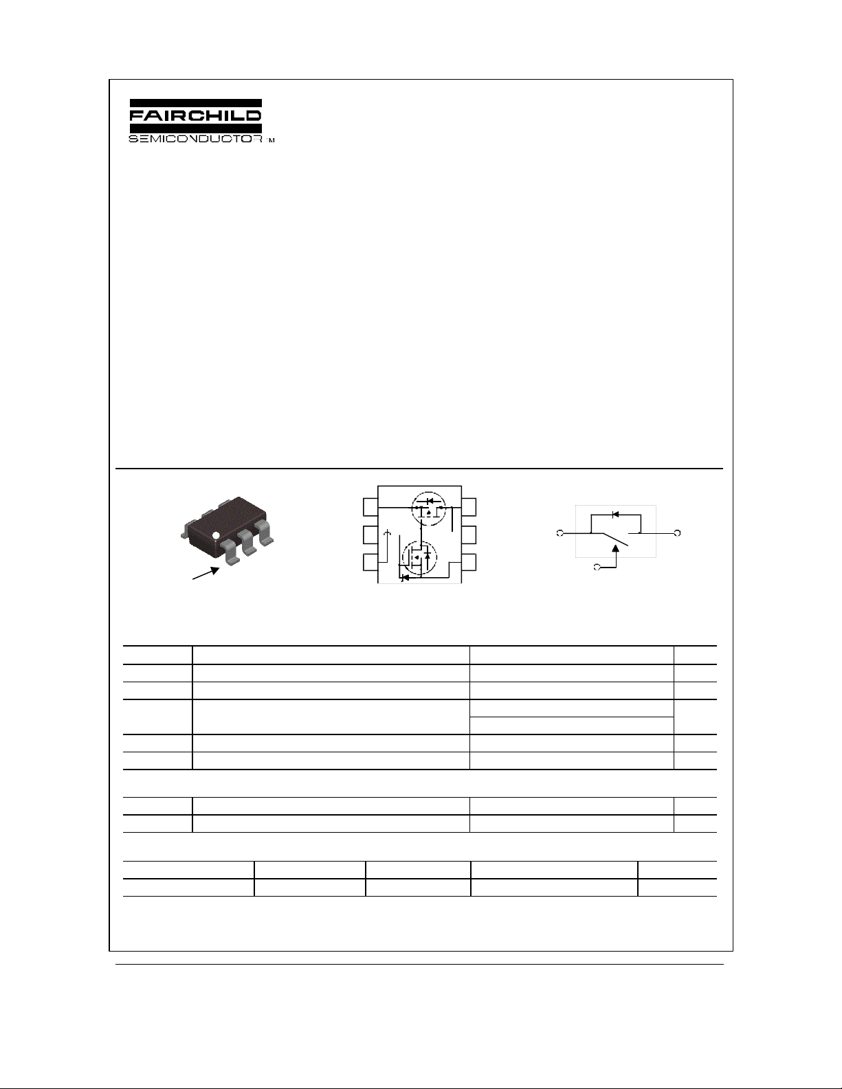
FDC6331L
FDC6331L
Integrated Load Switch
General Description
This device is particularly suited for compact power
management in portable electronic equipment where
2.5V to 8V input and 2.8A output current capability are
Features
• –2.8 A, –8 V. R
R
R
= 55 mΩ @ VGS = –4.5 V
DS(ON)
= 70 mΩ @ VGS = –2.5 V
DS(ON)
= 100 m Ω @ VGS = –1.8 V
DS(ON)
needed. This load switch integrates a s mall N-Channel
power MOSFET (Q1) that drives a large P-Channel
power MOSFET (Q2) in one tiny SuperSOTTM-6
package.
Applications
• Control MOSFET (Q1) includes Zener protection for
ESD ruggedness (>6KV Human body model)
• High performance trench technology for extremely
low R
DS(ON)
• Load switch
• Power management
D2
S1
D1
ON/OFF
G2
G1
S2
SuperSOT -6
TM
Pin 1
SuperSOT™-6
Absolute Maximum Ratings T
o
=25
C unless otherwise noted
A
Q2
Vout,C1
Q1
Equivalent Circuit
+ –IN OU
V
DROP
ON/OFF
Symbol Parameter Ratings Units
VIN Maximum Input Voltage ± 8 V
V
High level ON/OFF voltage range –0.5 to 8 V
ON/OFF
I
Load Current – Continuous (Note 1) –2.8 A
Load
– Pulsed –9
PD Maximum Power Dissipation (Note 1) 0.7 W
TJ, T
Operating and Storage Junction Temperature Range –55 to +150 °C
STG
Thermal Characteristics
R
θJA
R
θJC
Thermal Resistance, Junction-to-Ambient (Note 1) 180
Thermal Resistance, Junction-to-Case (Note 1) 60
°C/W
°C/W
Package Marking and Ordering Information
Device Marking Device Reel Size Tape width Quantity
.331 FDC6331L 7’’ 8mm 3000 units
2001 Fairchild Semiconductor Corporation FDC6331L Rev C(W)
FDC6331L
Electrical Characteristics T
= 25°C unless otherw ise noted
A
Symbol Parameter Test Conditions Min Typ Max Units
Off Characteristics
BVIN Vin Breakdown Voltage V
I
Zero Gate Voltage Drain Current VIN = 6.4 V, V
Load
IFL Leakage Current, Forward V
IRL Leakage Current, Reverse V
= 0 V, ID = –250 µA 8 V
ON/OFF
= 0 V –1 µA
ON/OFF
= 0 V, VIN = 8 V –100 nA
ON/OFF
= 0 V, VIN = –8 V 100 nA
ON/OFF
On Characteristics (Note 2)
V
R
R
Gate Threshold Voltage VIN = V
ON/OFF (th)
Static Drain–Source
DS(on)
On–Resistance (Q2)
Static Drain–Source
DS(on)
On–Resistance (Q1)
, ID = –250 µA 0.4 0.9 1.5 V
ON/OFF
VIN = 4.5 V, ID = –2.8A
VIN = 2.5 V, ID = –2.5 A
VIN = 1.8 V, ID = –2.0 A
VIN = 4.5 V, ID = 0.4A
VIN = 2.7 V, ID = 0.2 A
34
45
64
3.1
3.8
55
70
100
4
5
m Ω
Drain–Source Diode Characteristics and Maximum Ratings
IS Maximum Continuous Drain–Source Diode Forward Current –0.6 A
VSD Drain–Source Diode Forward
V
= 0 V, IS = –0.6 A (Note 2) –1.2 V
ON/OFF
Voltage
Notes:
1. R
is the sum of the junction-to-case and case-to-ambient thermal resistance where the case thermal reference is defined as the solder mounting
θJA
surface of the drain pins. R
2. Pulse Test: Pulse Width < 300µs, Duty Cycle < 2.0%.
is guaranteed by design while R
θJC
is determined by the user’s board design.
θJA
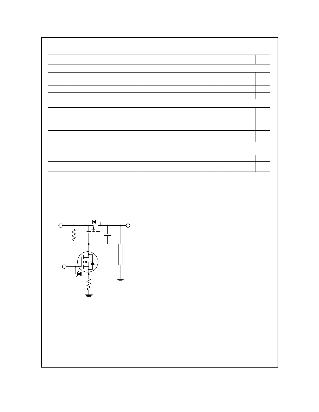
FDC6331L Load Switch Application Circuit
IN
Q2
OUT
Ω
R1
C1
Q1
LOAD
ON/OFF
R2
External Component Recommendation:
For additional in-rush current control, R2 and C1 can be added. For more information, see application note AN1030.
FDC6331L Rev C(W)
 Loading...