

Fairchild Semiconductor FDC6325L Datasheet
FDC6325L
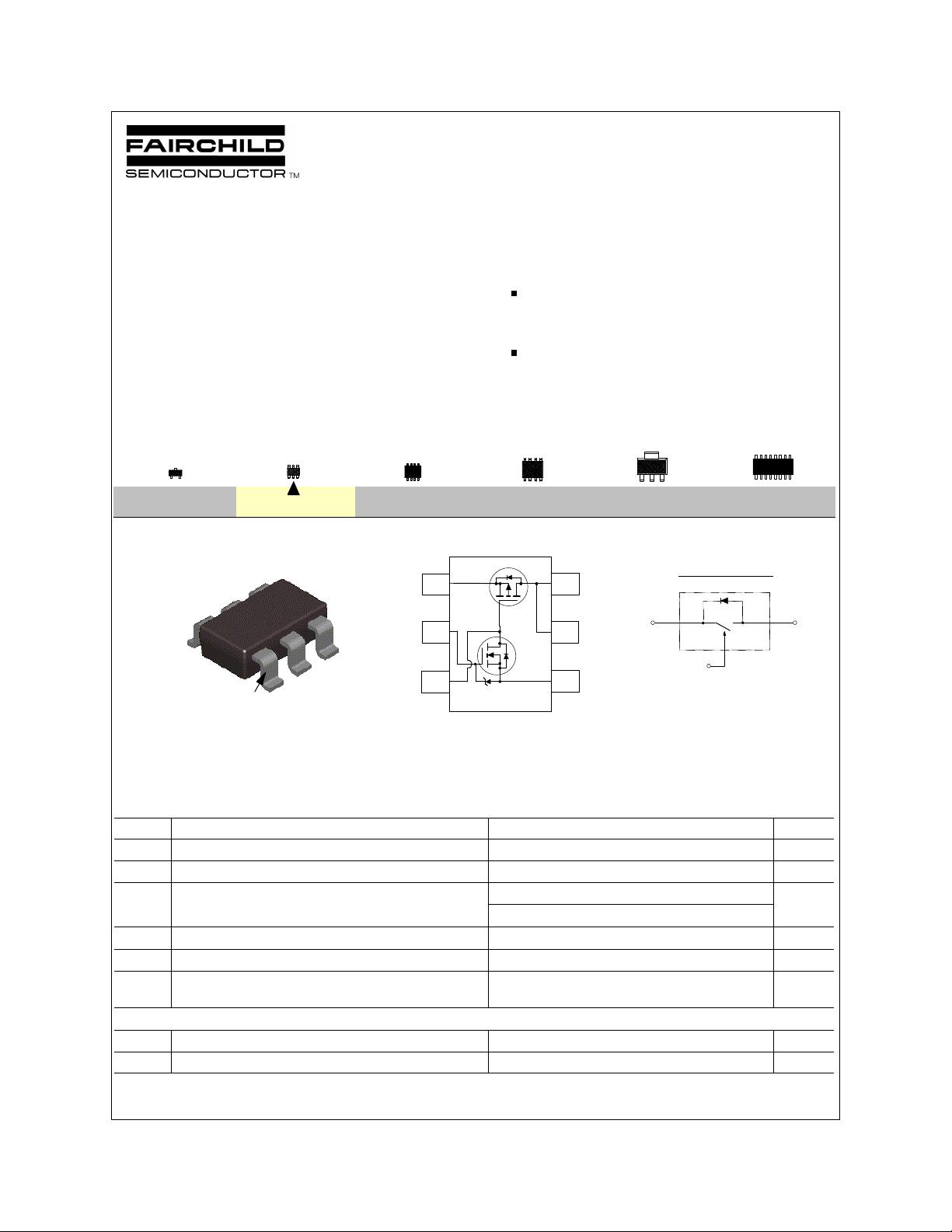
Integrated Load Switch
General Description Features
This device is particularly suited for compact power
management in portable electronic equipment where
2.5V to 8V input and 1.8A output current capability are
needed. This load switch integrates a small N-Channel
power MOSFET (Q1) which drives a large P-Channel
power MOSFET (Q2) in one tiny SuperSOTTM-6
package.
V
DROP
V
DROP
V
DROP
SuperSOTTM-6 package design using copper lead frame
for superior thermal and electrical capabilities.
=0.2V @ VIN=5V, IL=1.5A. R
=0.2V @ VIN=3.3V, IL=1.2A. R
=0.2V @ VIN=2.5V, IL=1A. R
August 1998
= 0.13Ω
(ON)
= 0.16Ω
(ON)
= 0.18Ω.
(ON)
SOT-23
SuperSOTTM-6
SuperSOTTM-8
SO-8
SOT-223
SOIC-16
IN
ON/OFF
EQUIVALENT CIRCUIT
V
DROP
+
-
Vout,C1
Q1
3
2
1
Vout,C1
R2
.325
1
pin
SuperSOT -6
Absolute Maximum Ratings T
TM
Vin,R1
4
ON/OFF
= 25°C unless otherwise noted
A
R1,C1
5
6
See Application Circuit
Q2
Symbol Parameter FDC6325L Units
V
V
I
L
IN
ON/OFF
Input Voltage Range 2.5 - 8 V
On/Off Voltage Range 1.5 - 8 V
Load Current - Continuous (Note 1) 1.8 A
- Pulsed (Note 1 & 3) 5
P
D
TJ,T
ESD Electrostatic Discharge Rating MIL-STD-883D Human Body
Maximum Power Dissipation (Note 2) 0.7 W
Operating and Storage Temperature Range -55 to 150 °C
STG
6 kV
Model (100pf/1500Ohm)
THERMAL CHARACTERISTICS
R
θJA
R
θJC
Thermal Resistance, Junction-to-Ambient (Note 2) 180 °C/W
Thermal Resistance, Junction-to-Case (Note 2) 60 °C/W
OUT
© 1998 Fairchild Semiconductor Corporation
FDC6325L Rev.D1
Electrical Characteristics (T
= 25°C unless otherwise noted)
A
Symbol Parameter Conditions Min Typ Max Units
OFF CHARACTERISTICS
I
FL
Forward Leakage Current VIN = 8 V, V
= 0 V 1 µA
ON/OFF
ON CHARACTERISTICS (Note 3)
V
DROP
R
(ON)
Conduction Voltage Drop
VIN = 5 V, V
VIN = 3.3 V, V
VIN = 2.5 V, V
= 3.3 V, IL = 1.5 A
ON/OFF
= 3.3 V, IL = 1.2 A
ON/OFF
= 3.3 V, IL = 1 A
ON/OFF
Q2 - Static On-Resistance VGS = -5 V, ID = -1.8 A
VGS = -3.3 V, ID = -1.6 A
VGS = -2.5 V, ID = -1.5 A
I
L
Notes:
1. VIN=8V, V
2. R
of the drain pins. R
3. Pulse Test: Pulse Width < 300µs, Duty Cycle < 2.0%.
Load Current
=8V, TA=25oC
ON/OFF
is the sum of the junction-to-case and case-to-ambient thermal resistance where the case thermal reference is defined as the solder mounting surface
JA
θ
is guaranteed by design while R
JC
θ
is determined by the user's board design.
CA
θ
V
= 0.13 V, VIN = 5 V, V
DROP
V
= 0.16 V, VIN = 3.3 V, V
DROP
V
= 0.2 V, VIN = 2.5V, V
DROP
ON/OFF
ON/OFF
ON/OFF
= 3.3 V
= 3.3 V
= 3.3 V
0.15 0.2 V
0.145 0.2
0.13 0.2
0.115 0.13
0.13 0.16
0.155 0.18
1 A
1
1
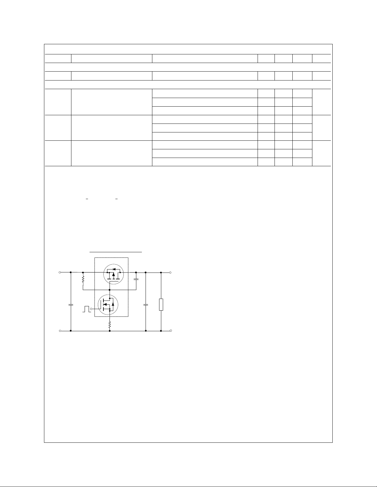
FDC6325L Load Switch Application
Ω
APPLICATION CIRCUIT
Q2
IN OUT
C1
LOAD
Co
ON/OFF
Ci
R1
Q1
R2
External Component Recommendation
For Co £ 1uF applications:
First select R2, 100 - 1kW, for Slew Rate control. C1 £ 1000pF can be added in addition to R2 for
further In-rush current control.
Then select R1 such that R1/R2 ratio maintains between 10 - 100. R1 is required to turn Q2 off.
For SPICE simulation, users can download a "FDC6325L.MOD" Spice model from Fairchild Web Site
at www.fairchildsemi.com
FDC6325L Rev.D1
 Loading...