Fairchild Semiconductor FDC6324L Datasheet

FDC6324L
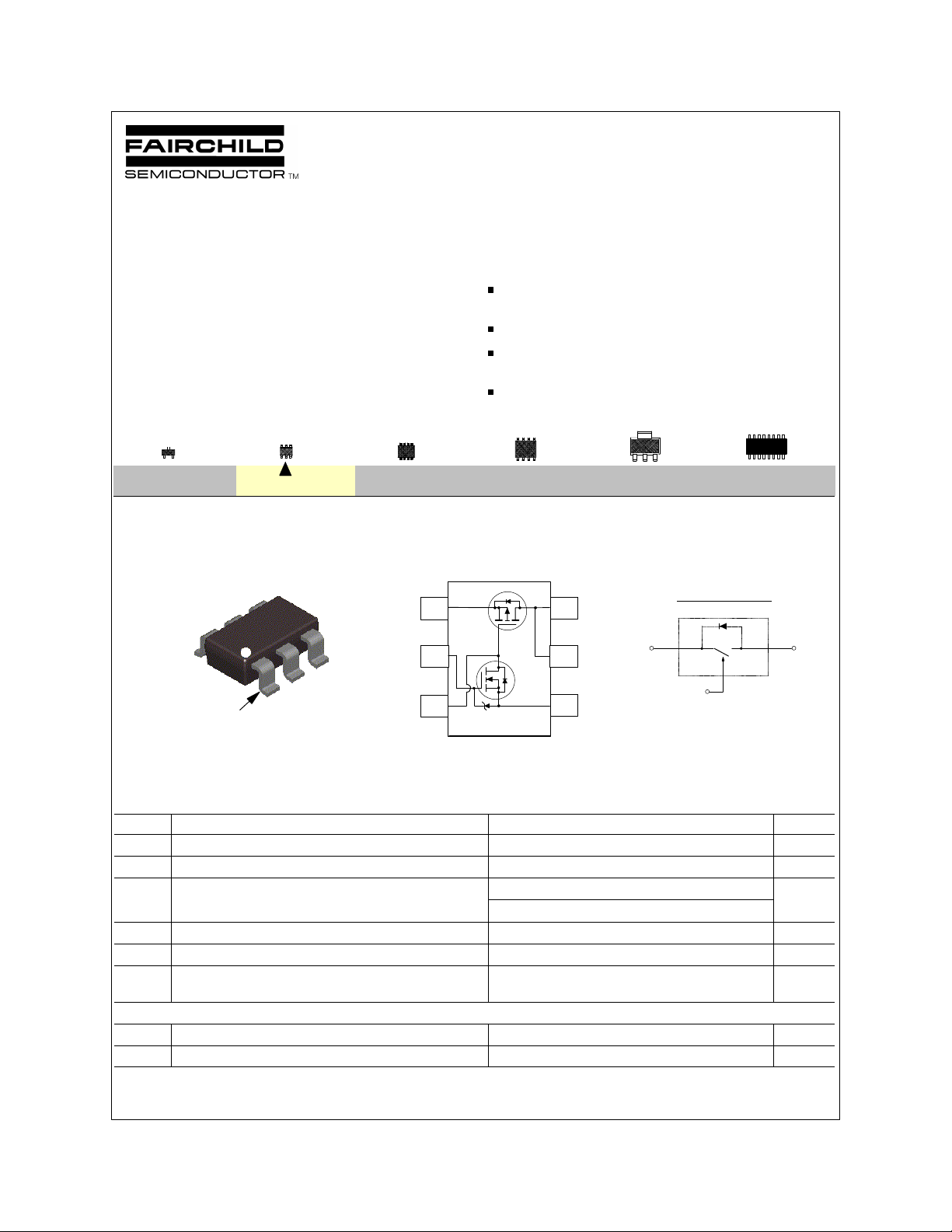
Integrated Load Switch
General Description Features
These Integrated Load Switches are produced using
Fairchild's proprietary, high cell density, DMOS
technology. This very high density process is
especially tailored to minimize on-state resistance and
provide superior switching performance. These devices
are particularly suited for low voltage high side load
switch application where low conduction loss and ease
of driving are needed.
V
DROP
V
DROP
High density cell design for extremely low on-resistance.
V
ON/OFF
>6KV Human Body Model.
SuperSOTTM-6 package design using copper lead frame for
superior thermal and electrical capabilities.
March 1999
=0.2V @ VIN=12V, IL=1A, V
=0.3V @ VIN=5V, IL=1A, V
Zener protection for ESD ruggedness.
ON/OFF
ON/OFF
=1.5 to 8V
=1.5 to 8V.
SOT-23
SuperSOT -6
pin
1
TM
SuperSOTTM-6
Absolute Operating Range T
SuperSOTTM-8
Vin,R1
4
ON/OFF
= 25°C unless otherwise noted
A
R1,C1
5
6
See Application Circuit
Q2
SO-8
Q1
3
2
1
Vout,C1
Vout,C1
R2
SOT-223
EQUIVALENT CIRCUIT
IN
ON/OFF
SOIC-16
V
DROP
+
-
Symbol Parameter FDC6324L Units
V
V
I
L
IN
ON/OFF
Input Voltage Range 3 - 20 V
ON/OFF Voltage Range 1.5 - 8 V
Load Current @ V
=0.5V - Continuous (Note 1) 1.5 A
DROP
- Pulsed (Note 1 & 3) 2.5
P
D
TJ,T
ESD Electrostatic Discharge Rating MIL-STD-883D Human Body
Maximum Power Dissipation (Note 2a) 0.7 W
Operating and Storage Temperature Range -55 to 150 °C
STG
6 kV
Model (100pf/1500Ohm)
THERMAL CHARACTERISTICS
R
θJA
R
JC
θ
Thermal Resistance, Junction-to-Ambient (Note 2a) 180 °C/W
Thermal Resistance, Junction-to-Case (Note 2) 60 °C/W
OUT
© 1999 Fairchild Semiconductor Corporation
FDC6324L Rev. D

Electrical Characteristics (T
= 25°C unless otherwise noted)
A
Symbol Parameter Conditions Min Typ Max Units
OFF CHARACTERISTICS
I
FL
I
RL
Forward Leakage Current VIN = 20 V, V
Reverse Leakage Current VIN = -20 V, V
= 0 V 1 µA
ON/OFF
= 0 V -1 µA
ON/OFF
ON CHARACTERISTICS (Note 3)
V
IN
V
ON/OFF
V
DROP
I
L
Notes:
1. VIN=20V, V
2. R
by design while R
P
D
Typical R
Input Voltage 3 20 V
On/Off Voltage 1.5 8 V
Conduction Voltage Drop @ 1A VIN = 10 V, V
VIN = 5 V, V
Load Current V
=8V, V
ON/OFF
is the sum of the junction-to-case and case-to-ambient thermal resistance where the case thermal reference is defined as the solder mounting surface of the drain pins. R
JA
θ
T
(t)
=
R
JA
θ
a. 180oC/W when mounted on a 2oz minimum copper pad.
=0.5V, TA=25oC
DROP
is determined by the user's board design.
CA
θ
−
J
θJ A
for single device operation using the board layouts shown below on FR-4 PCB in a still air environment:
−
T
T
T
A
=
(t)
R
θJ C
2
J
A
(t)
= I
×R
DS(ON)@T
D
+
(t)
R
θCA
J
= 0.2 V, VIN = 10 V, V
DROP
V
= 0.3 V, VIN = 5 V, V
DROP
= 3.3V 0.135 0.2 V
ON/OFF
= 3.3 V 0.215 0.3
ON/OFF
= 3.3 V 1 A
ON/OFF
= 3.3 V 1
ON/OFF
is guaranteed
JC
θ
2a
Scale 1 : 1 on letter size paper
3. Pulse Test: Pulse Width < 300µs, Duty Cycle < 2.0%
FDC6324L Rev. D

Typical Electrical Characteristics (T
= 25 OC unless otherwise noted )
A
0.5
T = 125°C
J
0.4
T = 25°C
0.3
DROP
0.2
V , (V)
0.1
0
0 1 2 3 4
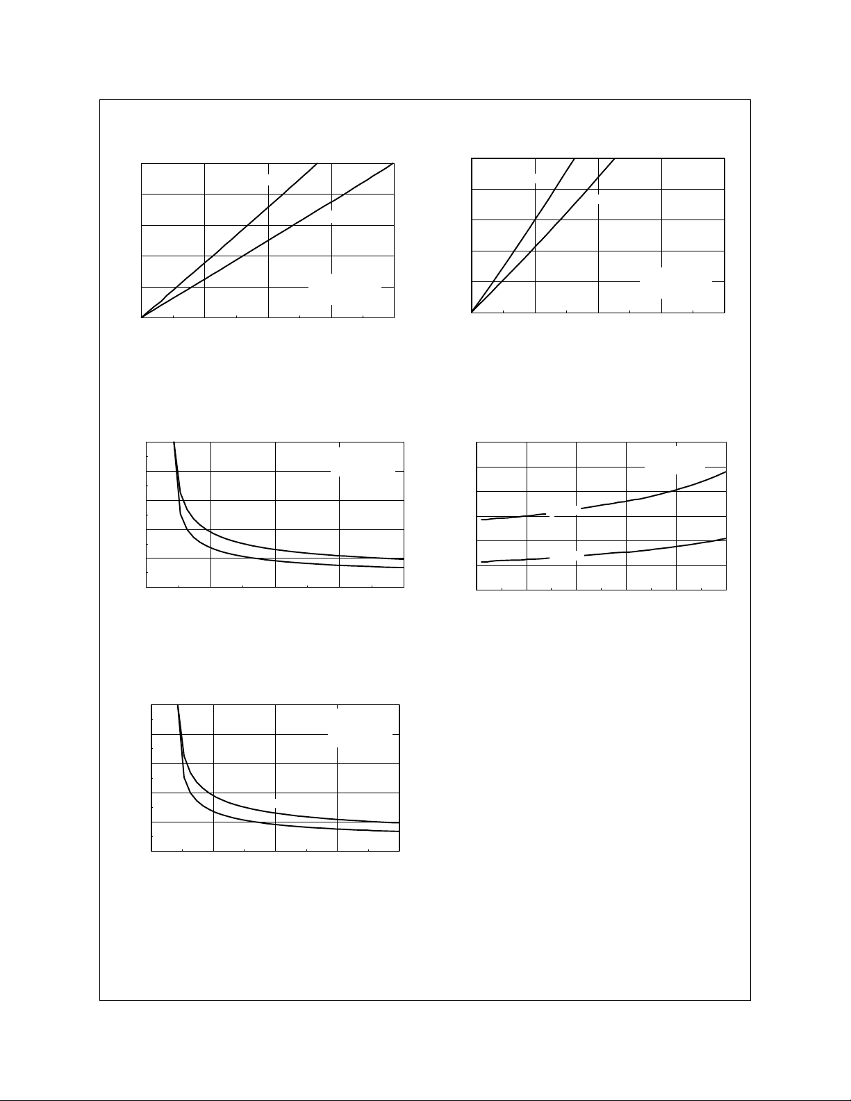
Figure 1. V
1
0.8
0.6
0.4
DROP
V (V)
0.2
0
1 2 3 4 5
DROP
I ,(A)
L
Versus IL at V
T = 125°C
J
T = 25°C
J
V (V)
IN
J
V = 12V
IN
V = 1.5 - 8V
ON/OFF
PW =300us, D≤ 2%
=12V.
IN
I = 1A
L
V = 1.5 - 8V
ON/OFF
PW =300us, D≤ 2%
0.5
T = 125°C
0.4
J
T = 25°C
J
0.3
DROP
0.2
V , (V)
V = 5V
IN
V = 1.5 - 8V
0.1
0
0 1 2 3 4
Figure 2. V
I (A)
L
Versus IL at VIN=5.0V.
DROP
0.45
0.4
)
0.35
T = 125°C
0.3
DS(ON), (Ohm
R
0.25
0.2
0.15
0 1 2 3 4 5
J
T = 25°C
J
I , (A)
L
ON/OFF
PW =300us, D≤ 2%
I = 1A
L
V = 5V
IN
PW =300us, D≤ 2%
Figure 3. V
1
0.8
0.6
0.4
(ON)
R ,(Ohm)
0.2
0
1 2 3 4 5
Versus V
DROP
T = 25°C
at IL=1A.
IN
I = 1A
L
V = 1.5 - 8V
ON/OFF
PW =300us, D≤ 2%
T = 125°C
J
J
V , (V)
IN
Figure 5. On Resistance Variation with
Input Voltage.
Figure 4. R
Versus IL at V
(ON)
=5.0V.
IN
FDC6324L Rev.D
 Loading...