

Fairchild Semiconductor FDC3512 Datasheet
FDC3512
80V N-Channel PowerTrench
MOSFET
FDC3512
February 2002
General Description
This N-Channel MOSFET has been designed
specifically to improve the overall efficiency of DC/DC
converters using either synchronous or conventional
switching PWM controllers. It has been optimized for
low gate charge, low R
and fast switching speed.
DS(ON)
Applications
• DC/DC converter
Features
• 3.0 A, 80 V R
R
• High performance trench technology for extremely
low R
• Low gate charge (13nC typ)
• High power and current handling capability
• Fast switching speed
DS(ON)
= 77 mΩ @ VGS = 10 V
DS(ON)
= 88 mΩ @ VGS = 6 V
DS(ON)
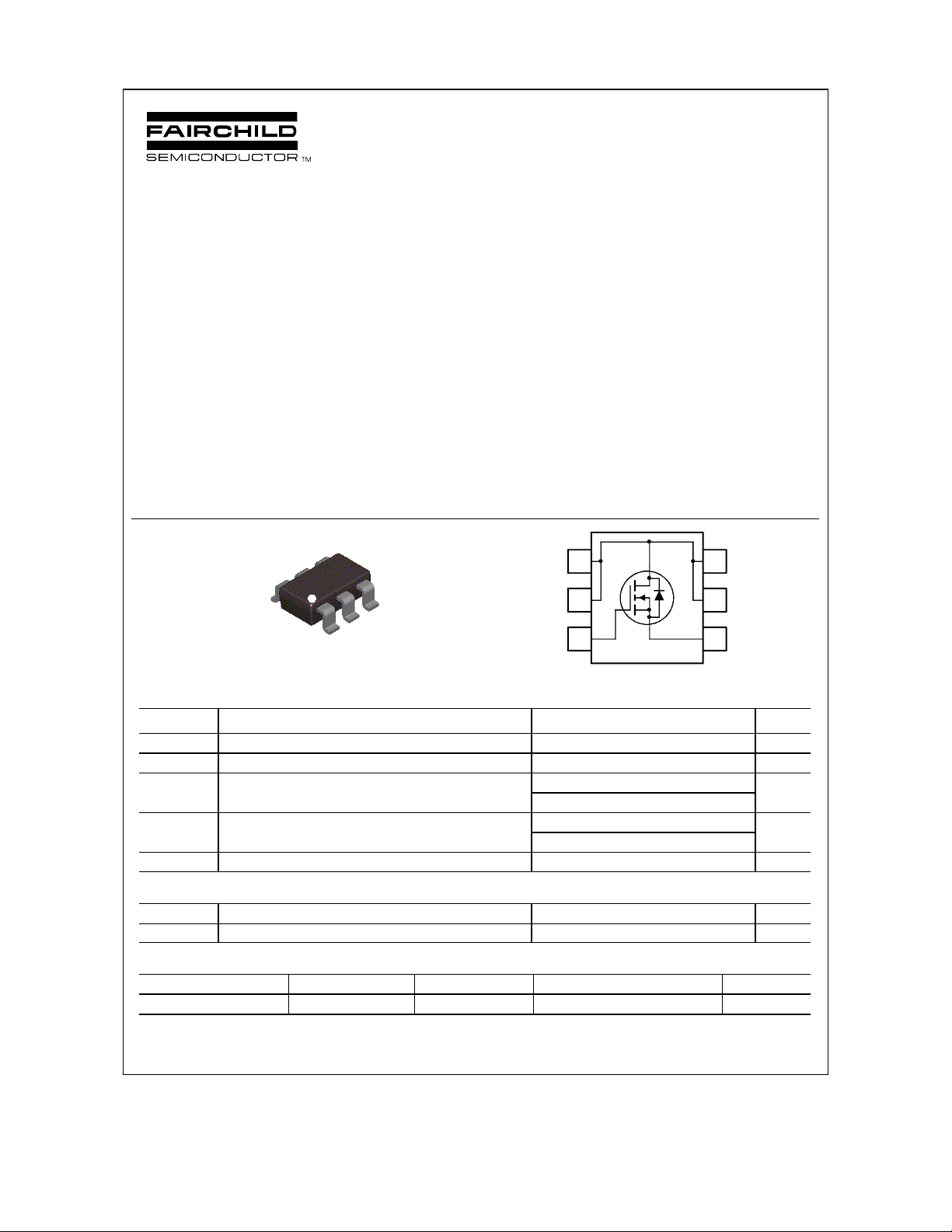
S
D
D
1
2
6
5
G
SuperSOT -6
TM
D
D
Absolute Maximum Ratings T
o
=25
C unless otherwise noted
A
3
4
Symbol Parameter Ratings Units
V
Drain-Source Voltage 80 V
DSS
V
Gate-Source Voltage
GSS
ID Drain Current – Continuous (Note 1a) 3.0 A
PD
TJ, T
STG
– Pulsed 20
Maximum Power Dissipation (Note 1a) 1.6 W
Operating and Storage Junction Temperature Range –55 to +150
(Note 1b)
± 20
0.8
V
°C
Thermal Characteristics
R
θJA
R
θJC
Thermal Resistance, Junction-to-Ambient
Thermal Resistance, Junction-to-Case
(Note 1a) 78
(Note 1) 30
Package Marking and Ordering Information
Device Marking Device Reel Size Tape width Quantity
2002 Fairchild Sem iconductor Corporation
.352 FDC3512 7’’ 8mm 3000 units
°C/W
°C/W
FDC3512 Rev B2 (W )
FDC3512
Electrical Characteristics T
= 25°C unless otherwise noted
A
Symbol Parameter Test Conditions Min Typ Max Units
Drain-Source Avalanche Ratings (Note 2)
W
Drain-Source Avalanche Energy Single Pulse, VDD = 40 V, ID=3.0 A 90 mJ
DSS
IAR Drain-Source Avalanche Current 3.0 A
Off Characteristics
BV
Drain–Source Breakdown Voltage
DSS
∆BVDSS
∆T
J
I
Zero Gate Voltage Drain Current VDS = 64 V, VGS = 0 V 1
DSS
I
Gate–Body Leakage, Forward VGS = 20 V, VDS = 0 V 100 nA
GSSF
I
Gate–Body Leakage, Reverse VGS = –20 V, VDS = 0 V –100 nA
GSSR
Breakdown Voltage Temperature
Coefficient
= 0 V, ID = 250 µA
V
GS
= 250 µA, Referenced to 25°C
I
D
80 V
80
mV/°C
µA
On Characteristics (Note 2)
V
Gate Threshold Voltage
GS(th)
∆VGS(th)
∆TJ
R
DS(on)
I
On–State Drain Current VGS = 10 V, VDS = 5 V 10 A
D(on)
Gate Threshold Voltage
Temperature Coefficient
Static Drain–Source
On Resistance
= VGS, ID = 250 µA
V
DS
= 250 µA, Referenced to 25°C
I
D
V
= 10 V, ID = 3.0 A
GS
V
= 6.0 V, ID = 2.8 A
GS
= 10 V, ID = 3.0 A;TJ = 125°C
V
GS
gFS Forward Transconductance VDS = 10 V, ID = 3.0 A 14 S
2 2.4 4 V
–6
56
61
97
77
88
141
mV/°C
mΩ
Dynamic Characteristics
C
Input Capacitance 634 pF
iss
C
Output Capacitance 58 pF
oss
C
Reverse Transfer Capacitance
rss
= 40 V, V
V
DS
f = 1.0 MHz
= 0 V,
GS
28 pF
Switching Characteristics (Note 2)
t
Turn–On Delay Time 7 14 ns
d(on)
tr Turn–On Rise Time 3 6 ns
t
Turn–Off Delay Time 24 28 ns
d(off)
tf Turn–Off Fall Time
Qg Total Gate Charge 13 18 nC
Qgs Gate–Source Charge 2.4 nC
Qgd Gate–Drain Charge
= 40 V, ID = 1 A,
V
DD
= 10 V, R
V
GS
V
= 40 V, ID = 3.0 A,
DS
V
= 10 V
GS
GEN
= 6 Ω
4 8 ns
2.8 nC
Drain–Source Diode Characteristics and Maximum Ratings
IS Maximum Continuous Drain–Source Diode Forward Current 1.3 A
VSD
t
rr
Qrr Diode Reverse Recovery Charge
Notes:
is the sum of the junction-to-case and case-to-ambient resistance where the case thermal reference is defined as the solder mounting surface of the drain
1. R
θJA
pins. R
a. 78°C/W when mounted on a 1in
b. 156°C/W when mounted on a minimum pad.
2. Pulse Test: Pulse Width ≤ 300 µs, Duty Cycl e ≤ 2.0%
Drain–Source Diode Forward
Voltage
Diode Reverse Recovery Time 28.2 nS
is guaranteed by design while R
θJC
2
pad of 2oz copper on FR-4 board.
is determined by the user's board design.
θCA
V
= 0 V, IS = 1.3 A (Note 2) 0.8 1.2 V
GS
I
= 3.0 A,
F
= 300 A/µs (Note 2)
d
iF/dt
48 nC
FDC3512 Rev B2(W )
 Loading...