

Fairchild Semiconductor FDB6644S Datasheet
JANUARY 2002
2002 Fairchild Sem iconductor Corporation
FDP6644S/FDB6644S Rev C1(W)
FDP6644S/FDB6644S
30V N-Channel PowerTrench
SyncFET™
General Description
This MOSFET is designed to replace a single MOSFET
and parallel Schottky diode in synchronous DC:DC
power supplies. This 30V MOSFET is designed to
maximize power conversion efficiency, providing a low
R
DS(ON)
and low gate charge. The FDP6644S includes
an integrated Schottky diode using Fairchild’s
monolithic SyncFET technology. The performance of
the FDP6644S/FDB6644S as the low-side switch in a
synchronous rectifier is indistinguishable from the
performance of the FDP6644/FDB6644 in parallel with
a Schottky diode.
Features
• 28 A, 30 V. R
DS(ON)
= 10 mΩ @ VGS = 10 V
R
DS(ON)
= 12 mΩ @ VGS = 4.5 V
• Includes SyncFET Schottky body diode
• Low gate charge (27nC typical)
• High performance trench technology for extremely
low R
DS(ON)
and fast switching
• High power and current handling capability
•
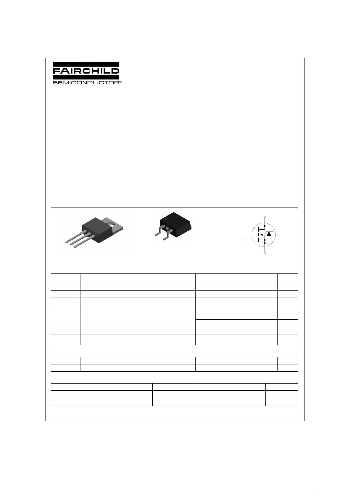
S
G
D
TO-220
FDP Series
D
G
S
TO-263AB
FDB Series
S
G
D
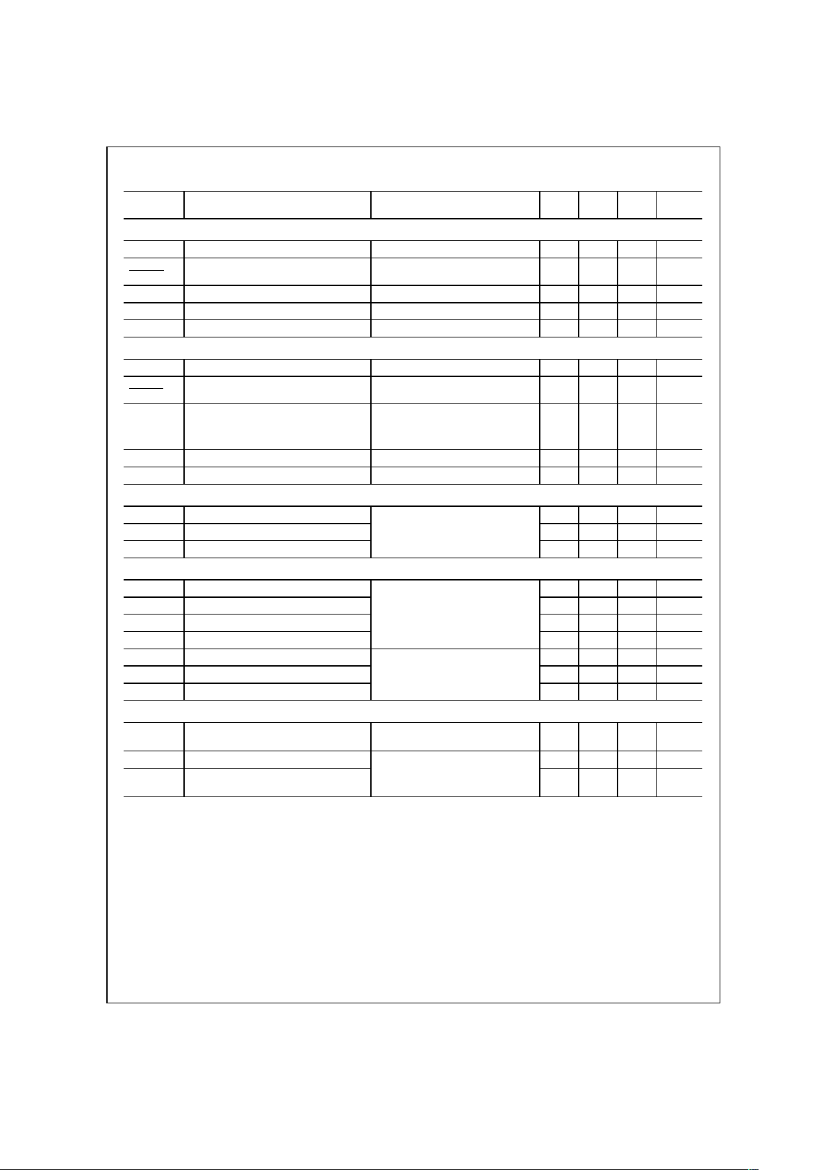
Absolute Maximum Ratings T
A
=25
o
C unless otherwise noted
Symbol Parameter Ratings Units
V
DSS
Drain-Source Voltage 30 V
V
GSS
Gate-Source Voltage
±16
V
ID Drain Current – Continuous (Note 1)
55
A
– Pulsed (Note 1)
150
PD
Total Power Dissipation @ T
C
= 25°C
60
W
Derate above 25°C
0.48
W/°C
TJ, T
STG
Operating and Storage Junction Temperature Range –65 to +125
°C
TL Maximum lead temperature for soldering purposes,
1/8” from case for 5 seconds
275
°C
Thermal Characteristics
R
θJC
Thermal Resistance, Junction-to-Case
2.1
°C/W
R
θJA
Thermal Resistance, Junction-to-Ambient
62.5
°C/W
Package Marking and Ordering Information
Device Marking Device Reel Size Tape width Quantity
FDB6644S FDB6644S 13’’ 24mm 800 units
FDP6644S FDP6644S Tube n/a 45
FDP6644S
/
FDB6644S
FDP6644S/FDB6644S Rev C1 (W)
Electrical Characteristics T
A
= 25°C unless otherwise noted
Symbol Parameter Test Conditions Min Typ Max Units
Off Characteristics
BV
DSS
Drain–Source Breakdown Voltage VGS = 0 V, ID = 1mA 30 V
∆BVDSS
∆T
J
Breakdown Voltage Temperature
Coefficient
I
D
= 10mA, Referenced to 25°C
23
mV/°C
I
DSS
Zero Gate Voltage Drain Current VDS = 24 V, VGS = 0 V 500 uA
I
GSSF
Gate–Body Leakage, Forward VGS = 16 V, VDS = 0 V 100 nA
I
GSSR
Gate–Body Leakage, Reverse VGS = –16 V VDS = 0 V –100 nA
On Characteristics (Note 2)
V
GS(th)
Gate Threshold Voltage VDS = VGS, ID = 1mA 1 1.3 3 V
∆VGS(th)
∆TJ
Gate Threshold Voltage
Temperature Coefficient
I
D
= 10mA, Referenced to 25°C
–9.5
mV/°C
R
DS(on)
Static Drain–Source
On–Resistance
VGS = 10 V, ID = 28 A
V
GS
= 4.5 V, ID = 25 A
V
GS
=10 V, ID =28 A, TJ=125°C
7
8
11.5
10
12
17
mΩ
I
D(on)
On–State Drain Current VGS = 10 V, VDS = 5 V 60 A
gFS Forward Transconductance VDS = 5 V, ID = 28 A 89 S
Dynamic Characteristics
C
iss
Input Capacitance 2851 pF
C
oss
Output Capacitance 540 pF
C
rss
Reverse Transfer Capacitance
V
DS
= 15 V, V
GS
= 0 V,
f = 1.0 MHz
196 pF
Switching Characteristics (Note 2)
t
d(on)
Turn–On Delay Time 12 21 ns
tr Turn–On Rise Time 11 20 ns
t
d(off)
Turn–Off Delay Time 53 85 ns
tf Turn–Off Fall Time
V
DS
= 15 V, ID = 1 A,
V
GS
= 10 V, R
GEN
= 6 Ω
17 30 ns
Qg Total Gate Charge 27 38 nC
Qgs Gate–Source Charge 7 nC
Qgd Gate–Drain Charge
V
DS
= 15 V, ID = 28 A,
V
GS
= 5 V
8 nC
Drain–Source Diode Characteristics
VSD Drain–Source Diode Forward
Voltage
VGS = 0 V, IS = 3.5 A (Note 1)
VGS = 0 V, IS = 7 A (Note 1)
0.48
0.6
0.7 V
trr Diode Reverse Recovery Time 21 nS
Qrr Diode Reverse Recovery Charge
I
F
= 28 A,
d
iF/dt
= 300 A/µs (Note 2)
34 nC
Notes:
1. Pulse Test: Pulse Width < 300µs, Duty Cycle < 2.0%
2. See “SyncFET Schottky body diode characteristics” below.
FDP6644S
/
FDB6644S
 Loading...