

Fairchild Semiconductor FDB5680 Datasheet
FDP5680/FDB5680
FDP5680/FDB5680 Rev. C
July 2000
2000 Fairchild Semiconductor International
FDP5680/FDB5680
60V N-Channel PowerTrench
TM
MOSFET
Features
40 A, 60 V. R
DS(ON)
= 0.020 Ω @ VGS = 10 V
R
DS(ON)
= 0.023 Ω @ VGS = 6 V.
Critical DC electrical parameters specified at evevated
temperature.
Rugged internal source-drain diode can eliminate the
need for an external Zener diode transient suppressor.
High performance trend technology for
extremely low R
DS(ON)
.
175°C maximum junction temperature rating.
Absolute Maximum Ratings T
C
= 25°C unless otherwise noted
Symbol Parameter
FDP5680 FDB5680
Units
V
DSS
Drain-Source Voltage 60 V
V
GSS
Gate-Source Voltage
±20
V
I
D
Maximum Drain Current - Continuous 40 A
- Pulsed 120
Total Power Dissipation @ TC = 25°C
65 W
P
D
Derate above 25°C
0.43
W/°C
TJ, T
STG
Operating and Storage Junction Temperature Range -65 to +175
°C
Thermal Characteristics
R
θ
JC
Thermal Resistance, Junction-to-Case 2.3
°C/W
R
θ
JA
Thermal Resistance, Junction-to-Ambient 62.5
°C/W
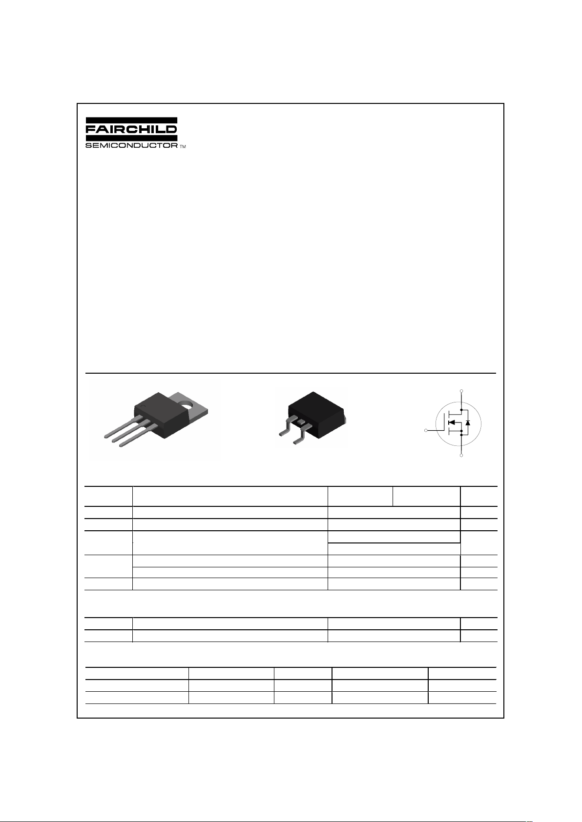
Package Marking and Ordering Information
Device Marking Device Reel Size Tape Width Quantity
FDB5680 FDB5680 13’’ 24mm 800
FDP5680 FDP5680 Tube N/A 45
S
D
G
S
G
D
TO-220
FDP Series
D
G
S
TO-263AB
FDB Series
General Description
This N-Channel MOSFET has been designed specifically
to improve the overall efficiency of DC/DC converters
using either synchronous or conventional switching PWM
controllers.
These MOSFETs feature faster switching and lower gate
charge than other MOSFETs with comparable R
DS(on)
specifications resulting in DC/DC power supply designs
with higher overall efficiency.
FDP5680/FDB5680
FDP5680/FDB5680 Rev. C
Electrical Characteristics
Tc = 25°C unless otherwise noted
Symbol Parameter Test Conditions Min Typ Max Units
Drain-Source Avalanche Ratings
(Note1)
W
DSS
Single Pulse Drain-Source
Avalanche Energy
VDD = 30 V, ID = 40A 90 mJ
I
AR
Maximum Drain-Source Av al anche Current 40 A
Off Characteristics
BV
DSS
Drain-Source Breakdown Voltage VGS = 0 V, ID = -250 µA60 V
∆
BV
DSS
∆
T
J
Breakdown Voltage Temperature
Coefficient
ID = -250
A, Referenced to 25°C60 mV/
°
C
I
DSS
Zero Gate Voltage Drain Current VDS = 48 V, VGS = 0 V 1
µ
A
I
GSSF
Gate-Body Leakage Current,
Forward
VGS = 20 V, VDS = 0 V 100 nA
I
GSSR
Gate-Body Leakage Current,
Reverse
VGS = -20 V, VDS = 0 V -100 nA
On Characteristics
(Note 1)
V
GS(th)
Gate Threshold Voltage VDS = VGS, ID = 250 µA22.54V
∆
V
GS(th)
∆
T
J
Gate Threshold Voltage
Temperature Coefficient
ID = -250
A, Referenced to 25°C-6.4 mV/
°
C
R
DS(on)
Static Drain-Source
On-Resistance
VGS = 10 V, ID = 20 A,
V
GS
= 10 V, ID = 20 A,TJ = 125°C
V
GS
= 6 V, ID = 19 A
0.016
0.022
0.018
0.020
0.035
0.023
Ω
I
D(on)
On-State Drain Current VGS = 10 V, VDS = 5 V 20 A
g
FS
Forward Transconductance VDS = 5 V, ID = 20 A 43 S
Dynamic Characteristics
C
iss
Input Capacitance 1850 pF
C
oss
Output Capacitance 230 pF
C
rss
Reverse Transfer Capacitance
V
DS
= 25 V, VGS = 0 V,
f = 1.0 MHz
95 pF
Switching Characteristics
(Note 1)
t
d(on)
Turn-On Delay Time 15 27 ns
t
r
Turn-On Rise Time 9 18 ns
t
d(off)
Turn-Off Delay Time 35 56 ns
t
f
Turn-Off Fall Time
V
DD
= 30 V, ID = 1 A,
V
GS
= 10 V, R
GEN
= 6
Ω
16 26 ns
Q
g
Total Gate Charge 33 46 nC
Q
gs
Gate-Source Charge 6.5 nC
Q
gd
Gate-Drain Charge
V
DS
= 30 V, ID = 20 A
V
GS
= 10 V
7.5 nC
Drain-Source Diode Characteristics and Maximum Ratings
I
S
Maximum Continuous Drain-Source Diode Forward Current
(Note 1)
40 A
V
SD
Drain-Source Diode Forward
Voltage
VGS = 0 V, IS = 20 A
(Note 1)
0.9 1.2 V
Note:
1. Pulse Test: Pulse Width ≤ 300 µs, Duty Cycle ≤ 2.0%
FDP5680/FDB5680
FDP5680/FDB5680 Rev. C
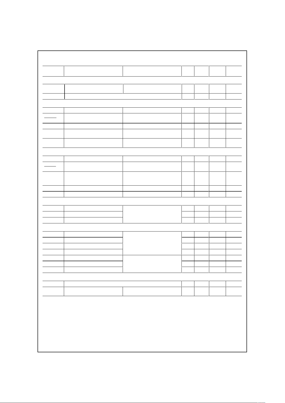
Typical Characteristics
Figure 1. On-Region Characteristics. Figure 2. On-Resistance Variation with
Drain Current and Gate Voltage.
Figure 3. On-Resistance Variation
with Temperature.
Figure 4. On-Resistance Variation
with Gate-to-Source Voltage.
Figure 5. Transfer Characteristics.
Figure 6. Body Diode Forward Voltage
Variation with Source Current
and Temperature.
0
10
20
30
40
50
60
70
80
01234
V
DS
, DRAIN-SOURCE VOLTAGE (V)
I
D
, DRAIN-SOURCE CURRENT (A)
VGS = 10V
4.0V
5.0V
4.5V
6.0V
0.8
1
1.2
1.4
1.6
1.8
2
2.2
0 1020304050607080
I
D
, DRAIN CURRENT (A)
R
DS(ON)
, NORMALIZED
DRAIN-SOURCE ON-RESISTANCE
VGS = 4.0V
10V
5.0V
7.0V
4.5V
6.0V
0.4
0.6
0.8
1
1.2
1.4
1.6
1.8
2
-50 -25 0 25 50 75 100 125 150
T
J
, JUNCTION TEMPERATURE (oC)
R
DS(ON)
, NORMALIZED
DRAIN-SOURCE ON-RESISTA N C E
ID = 20A
V
GS
= 10V
0
0.01
0.02
0.03
0.04
0.05
345678910
V
GS
, GATE TO SOURCE VOLTAGE (V)
R
DS(ON)
, ON-RESISTANCE (OHM)
ID = 20A
TA = 125oC
TA = 25oC
0
10
20
30
40
50
60
23456
V
GS
, GATE TO SOURCE VOLTAGE (V)
I
D
, DRAIN CURRENT (A)
TA = -55oC
25oC
125oC
VDS = 5V
0.0001
0.001
0.01
0.1
1
10
100
00.20.40.60.811.21.4
V
SD
, BODY DIODE FORWARD VOLTAGE (V)
I
S
, REVERSE DRAIN CURRENT (A)
TA = 125oC
25oC
-55oC
VGS = 0V
FDP5680/FDB5680
FDP5680/FDB5680 Rev. C
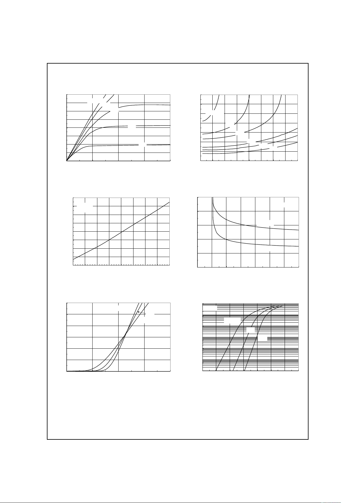
Typical Characteristics (continued)
Figure 7. Gate-Charge Characteristics. Figure 8. Capacitance Characteristics.
Figure 9. Maximum Safe Operating Area. Figure 10. Single Pulse Maximum
Power Dissipation.
Figure 11. Transient Thermal Response Curve.
0
2
4
6
8
10
0 5 10 15 20 25 30 35
Q
g
, GATE CHARGE (nC)
V
GS
, GATE-SOURCE VOLTAGE (V)
ID = 20A VDS = 10V
20V
30V
0
500
1000
1500
2000
2500
0 102030405060
V
DS
, DRAIN TO SOURCE VOLTAGE (V)
CAPACITANCE (pF)
C
ISS
C
RSS
C
OSS
f = 1MHz
V
GS
= 0 V
0
300
600
900
1200
1500
0.0001 0.001 0.01 0.1 1 10
SINGLE PULSE TIME (SEC)
POWER (W)
SINGLE PULSE
R
θJC
= 2.3oC/W
T
C
= 25oC
0.1 0.5 1 10 100 1000 3000 10000
0.03
0.05
0.1
0.2
0.3
0.5
1
t ,TIME (ms)
TRANSIENT THERMAL RESISTANCE
Single Pulse
D = 0.5
0.1
0.05
0.02
0.2
Duty Cycle, D = t /t
1 2
R (t) = r(t) * R
R =2.3 °C/W
θ
JC
θ
JC
θ
JC
T - T = P * R (t)
θ
JCC
J
P(pk)
t
1
t
2
r
(
t
)
,
N
O
R
M
A
L
I
Z
E
D
E
F
F
E
C
T
I
V
E
1
0.1
1
10
100
1000
0.1 1 10 100
DC
10s
1s
100ms
10ms
1ms
RDS(ON) LIMIT
VGS = 10V
SINGLE PULSE
R
θ
JC
= 2.3oC/W
T
C
= 25oC
I
D
DRAIN CURRENT (A)
VDS, DRAIN-SOURCE VOLTAGE (V)
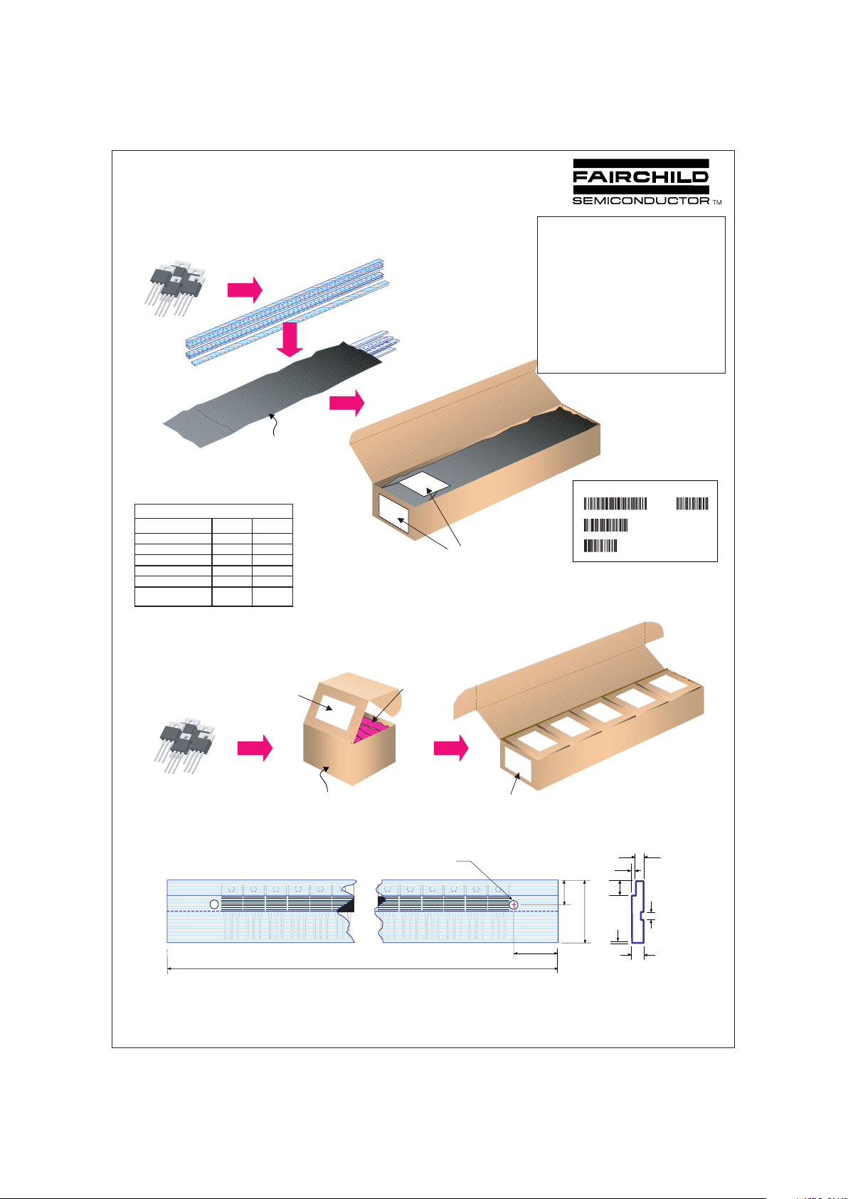
TO-220 Tape and Reel Data and Package Dimensions
August 1999, Rev. B
0.165
TO-220 Tube Packing
Configuration: Figure 1.0
Note/Comments
Packaging Option
TO-220 Packaging Information
Stan dard
(no fl ow code )
Packaging type
Rail/Tube
Qty per Tube/Box
45
Box Dimension (mm)
530x130x83
Max qty per Box
1,080
Weight per unit (gm)
1.4378
S62Z
BULK
300
114x102x51
1,500
1.4378
FSCINT Label
FSCINT Label
114mm x 102mm x 51mm
EO70 Immediate Box
530mm x 130mm x 83mm
Intermediate box
300 units per
EO70 box
5 EO70 boxes per per
Intermed iate Box
1500 units maximum
quantity per intermediate box
Anti-static
Bubbl e Sheets
45 units per Tube
Conduct ive Plastic Bag
1080 units maximum
quantity per box
530mm x 130mm x 83mm
Intermediate box
FSCINT Label
12 Tubes per Bag
Note: All dim ensi ons are in inches
F
9852
NDP4060L
F
9852
NDP4060L
F
9852
NDP4060L
F
9852
NDP4060L
F
9852
NDP4060L
F
9852
NDP4060L
F
9852
NDP4060L
F
9852
NDP4060L
F
9852
NDP4060L
F
9852
NDP4060L
F
9852
NDP4060L
F
9852
NDP4060L
1.300
±.015
0.080
0.032
±.003
0.275
0.275
0.160
0.800
0.450
±.030
20.000
+0.031
-0.065
0.123
+0.001
-0.003
LOT:
CBVK741B019
NSID:
FDP7060
D/C1:
D9842
SPEC REV:
B2
SPEC:
QTY:
1080
QA REV:
FAIRCHILD SEMICONDUCTOR CORPORATION
HTB:B
(FSCINT)
FSCINT Label sample
TO-220 Tube
Configuration: Figure 4.0
TO-220 Packaging
Information: Figure 2.0
TO-220 bulk Packing
Configuration: Figure 3.0
2 bags per Box
Packaging Description:
TO-220 parts are shipp ed normally in tube. The tub e is
made of PVC plas tic t reated wi th anti -stati c agent .These
tubes in s tandard opt ion are placed in side a di ssipativ e
plastic bag, barcode labeled, and placed in side a box
made of r ecy clab le cor rug ate d pape r. On e bo x co nt ain s
tw o ba gs m ax im um (se e fi g. 1. 0). A nd on e or se ver al o f
these boxes are placed ins ide a labeled shipp ing box
wh ic h c o m es in d i f f er en t si z es de pe ndi n g o n t h e nu m be r
of parts shipped. The other option comes in bulk as
described in the Packagin g In fo rm atio n table. The unit s in
this op tion are plac ed inside a s mall box laid w ith antistatic bu bble sheet. These smaller box es are indiv idually
labeled and plac ed inside a lar ger box (see fig. 3.0).
These larger or int ermediate boxes then w ill be placed
finally ins ide a labeled ship ping box whic h st ill co mes in
diff erent sizes depending on the num b er of units shipped.
 Loading...