

Fairchild Semiconductor FAN8725 Datasheet

FAN8725 (KA3025)
Spindle Motor and 5-Channel Motor Driver
www.fairchildsemi.com
Features
Common
• Built-in thermal shutdown circuit (TSD)
• Built-in power save circuit
• 3 Independent voltage source
• Corresponds to 3.3V or 5V DSP
Spindle
• Built-in hall bias
• Built-in FG signal output circuit
• Built-in rotational direction detecting circuit
• Built-in protection circuit for reverse rotation
• Built-in short brake circuit
BTL (5-channel)
• Built-in 5-CH balanced transformerless (BTL) driver
• Built-in Level shift circuit
• Independent voltage sources
• VM2 = CH1,CH2 / VM3 = CH3, CH4 ,CH5
Description
The FAN8725 is a monolithic IC suitable for a 3-phase
BLDC spindle motor driver and 5-ch motor drivers which
drives the focus actuator, tracking actuator, loading motor,
stepping motor driver of the CD-media systems.
48-QFPH-1414
Typical Applications
• Compact disk R OM (CD-ROM)
• Compact disk RW (CD-RW)
• Digital video disk ROM (DVD-ROM)
• Digital video disk RAM (DVD-RAM)
• Digital video disk Player (DVDP)
• Other compact disk media
©2000 Fairchild Semiconductor International
Ordering Information
Device Package Operating Temp.
FAN8725 48-QFPH-1414 −35°C ~ +85°C
Rev. 1.0.1
March. 2000.
1

FAN8725 (KA3025)
Pin Assignments
VH
48 47 46 45 44 43 42 41 40 39 38 37
PC1
EC
ECR
PS
SB
VREF
SVCC2
VM3
OUT5
IN5
PGND3
H1+
H1-
H2+
H2-
H3+
H3-
FG
DIR
SVCC1
VM1
CS1
PGND1
1
2
3
4
5
6
DO5 -
36
35
DO5+
DO4 -
34
DO4+
32
DO3 -
32
DO3+
31
FAN8725
7
8
9
10
11
12
30
PGND2
DO2 -
29
DO2+
28
DO1 -
27
26
DO1+
OUT1
25
13 14 15 16 17 18 19 20 21 22 23 24
A2
A3
A1
SGND2
OUT4
IN4
OUT3
IN3
IN2
OUT2
VM2
2
IN1

Pin Definitions
Pin Number Pin Name I/O Pin Function Description
1 H1- I Hall 1(-) input
2 H1+ I Hall 1(+) input
3 H2+ I Hall 2(-) input
4 H2- I Hall 2(+) input
5 H3+ I Hall 3(-) input
6 H3- I Hall 3(+) input
7 FG O Frequency Generator output
8 DIR O Rotation direction output
9 SVCC1 - Spindle Signal supply voltage
10 VM1 - Spindle power supply
11 CS1 I Spindle current sense
12 PGND1 - Spindle power ground
13 A1 O 3-phase output1
14 A2 O 3-phase output2
15 A3 O 3-phase output3
16 SGND2 - CH signal ground
17 IN4 I OP-Amp CH 4 input(-)
18 OUT4 O OP-Amp CH 4 output
19 IN3 I OP-Amp CH 3 input(-)
20 OUT3 O OP-Amp CH 3 output
21 IN2 I OP-Amp CH 2 input(-)
22 OUT2 O OP-Amp CH 2 output
23 VM2 - CH1/CH2 power supply
24 IN1 I OP-Amp CH 1 input(-)
25 OUT1 O OP-Amp CH 1 output
26 DO1+ O Channel 1 output (+)
27 DO1 - O Channel 1 output (−)
28 DO2+ O Channel 2 output (+)
29 DO2 - O Channel 2 output (−)
30 PGND2 - CH1/CH2 power ground
31 DO3+ O Channel 3 output (+)
32 DO3 - O Channel 3 output (−)
33 DO4+ O Channel 4 output (+)
FAN8725 (KA3025)
3

FAN8725 (KA3025)
Pin Definitions (Continued)
Pin Number Pin Name I/O Pin Function Description
34 DO4 - O Channel 4 output (−)
35 DO5+ O Channel 5 output (+)
36 DO5- O Channel 5 output (−)
37 PGND3 - CH3/CH4/CH5 power ground
38 IN5 I OP-Amp CH 5 input(-)
39 OUT5 O OP-Amp CH 5 output
40 VM3 - CH3/CH4/CH5 power supply
41 SVCC2 - CH Signal supply voltage
42 VREF I BTL reference voltage
43 SB I Short brake
44 PS I Power save
45 ECR I Torque control reference
46 EC I Torque control
47 PC1 - Phase compensation capacitor
48 VH I Hall bias
Notes:
BTL drive part symbol(+,- outputs of drives) is determined according to the polarity of input pin.
(For example, if the voltage of pin 24 is high, the output of pin 26 is high)
4

Internal Block Diagram
FAN8725 (KA3025)
H1+
H1 -
H2+
H2 -
H3+
H3 -
FIN(GND)
FG
DIR
PC1
EC
CS1VM
ECR
454647
Absolute Values
Output
Current Limit
VH
48
Hall
1
2
3
4
5
Bias
Hall Amp
SB
PS
4344 42 41 40 39 38 37
Current
Sense Amp
FIN(GND)
VREF
SVCC2
VM3
OUT5
CH5
X8
CH4
X8
IN5
PGND3
36
35
34
33
32
DO5 -
DO5+
DO4 -
DO4+
DO3 -
CH3
6
Detection
FG
Generator
7
8
Logic
Reverse
Rotation
Short
Brake
VM3
VM2
R
R
VM3
R
R
VM2
X8
CH2
X5
VM3
VM2
31
30
29
DO3+
FIN(GND)
PGND2
DO2 -
SVCC1
VM1
CS1
PGND1
10
11
12
9
Distributor
Driver
13 16
14 18
A1
A2
15
A3
17
IN4
SGND2
OUT4
FIN(GND)
5
19 20
IN3
21
OUT3
IN2
CH1
X5
22 23
OUT2
VM2
24
IN1
28
27
26
25
DO2+
DO1 -
DO1+
OUT1
FAN8725 (KA3025)
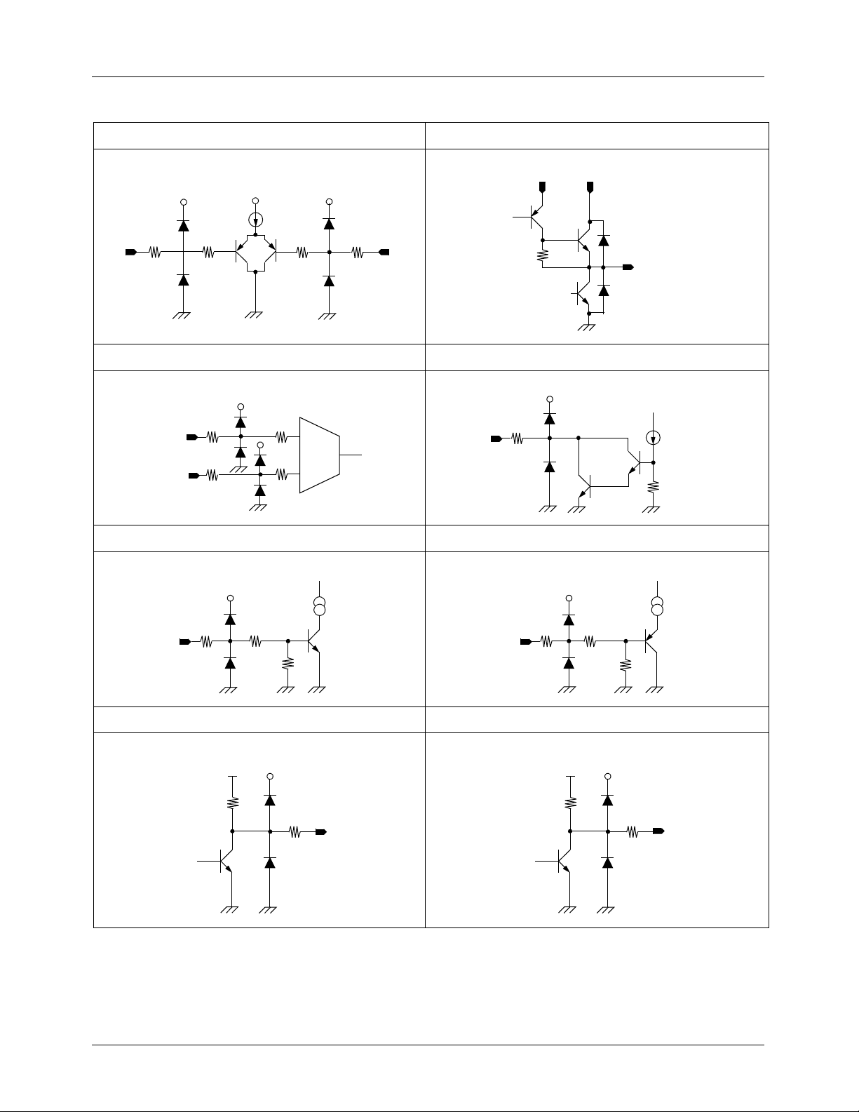
Equivalent Circuits (Spindle Part)
HALL INPUT DRIVER OUTPUT
Pin
10
Pin
11
Pin
1,3,5
22.5Ω
1KΩ 1KΩ
22.5Ω
Pin
2,4,6
15KΩ
TORQUE CONTROL INPUT HALL BIAS INPUT
Pin 45
22.5Ω
22.5Ω
Pin 46
1KΩ
1KΩ
+
Pin 48
5Ω
-
POWER SAVE INPUT SHORT BRAKE INPUT
Pin 44
22.5Ω
40KΩ
30KΩ
Pin 43
22.5Ω
1KΩ
Pin 13,14,15
100KΩ
20KΩ
FG OUTPUT DIR OUTPUT
10KΩ
Vcc
22.5Ω
Pin
7
Vcc
30KΩ
6
22.5Ω
Pin 8
 Loading...