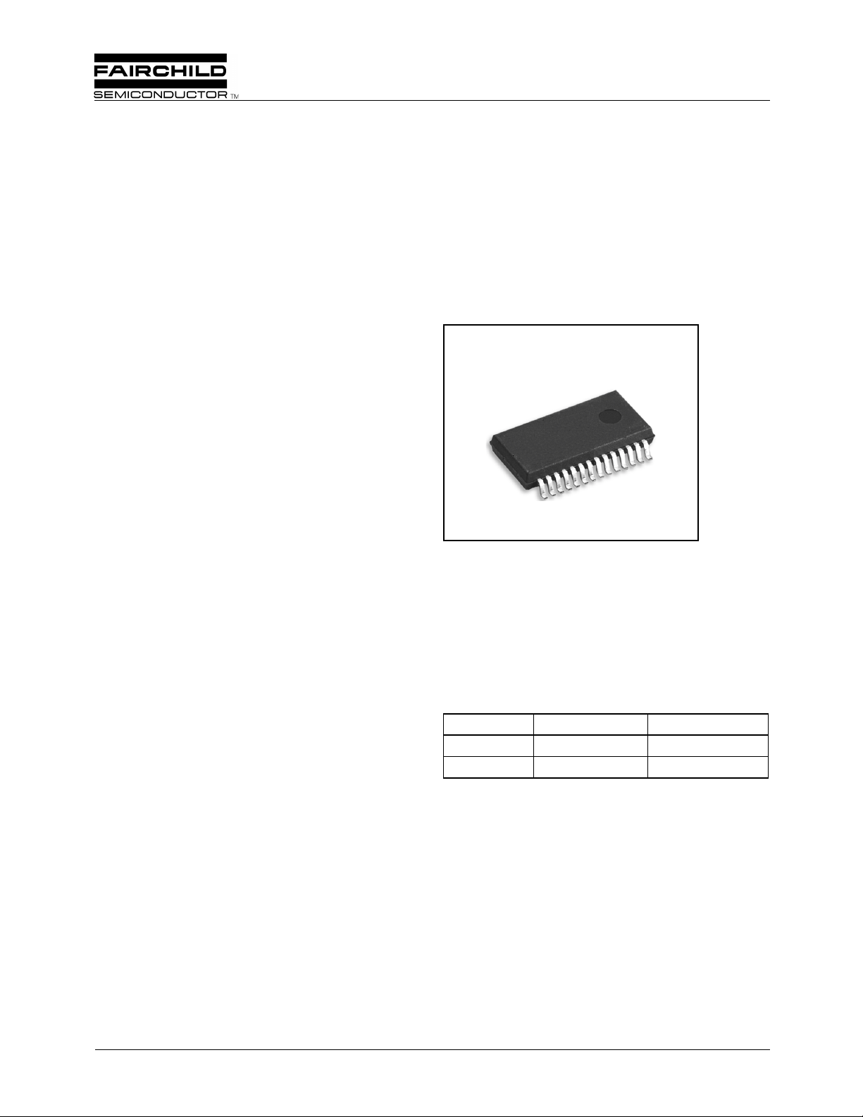
Fairchild Semiconductor FAN8486D Datasheet

FAN8486D (KA3086D)
2-Phase BLDC Motor Driver
www.fairchildsemi.com
Features
• Drives the BLDC motor using 2 hall sensors.
• 2-phase, full-wave drive method
• Built-in thermal shutdown (TSD) circuit
• Controls the motor speed through voltage
• Built-in bandgap circuit
• Built-in frequency Generator (FG) & Phase Generator
(PG) amplifier & comparator.
Descripiton
The FAN8486D is a monolithic integrated circuit, and it is
suitable for drum motor driver of VCR system.
28-SSOP-300SG
Typical Applications
• Video cassette recorder (VCR) cylinder (drum) motor
• Other 2-phase BLDC motor
©2000 Fairchild Semiconductor International
Ordering Information
Device Package Operating Temp.
FAN8486D 28-SSOP-300SG −25°C ~ +75°C
FAN8486DTF 28-SSOP-300SG −25°C ~ +75°C
Rev. 1.0.1
February. 2000.

FAN8486D (KA3086D)
Pin Assignments
SGND
VCTL
H2P
FGAMPOUT
FGIN
FGOUT
VREG
PG(V25)
FG(V25)
PGAMPOUT
PGIN
1920212223242526
H2N
PGOUT
1428 27
161718
H1N
15
FAN8486D
23
14
NC
PVCC2
45 7 9
NC
NC
6
OUT2P
PGND2
8
OUT2N
OUT1P
PGND1
11
10
OUT1N
12
NC
PVCC1
14
13
H1P
SVCC
2
Rev. 1.0.1
February. 2000.

Pin Definitions
Pine Number Pin Name I/O Pin Function Description
1 PVCC2 - Power supply voltage2
2NC -3NC -4NC -5 OUT2P O Output drive 2(P)
6 PGND2 O Power ground 2
7 OUT2N O Output drive 2(N)
8 OUT1P O Output drive 1(P)
9 PGND1 O Power ground 1
10 OUT1N - Output drive 1(N)
11 NC - 12 PVCC1 - Power supply voltage1
13 SVCC - Signal supply voltage
14 H1P I Hall signal input 1P
15 H1N I Hall signal input 1N
16 H2P I Hall signal input 2P
17 H2N I Hall signal input 2N
18 PGOUT O Phase generate output
19 PGAMPOUT O Phas e generate amp. output
20 PGIN I P hase generate input
21 PG(V25) - Reference voltage for PG
22 VREG - Regulated voltage
23 FG(V25) - Reference voltage for FG
24 FGIN I Frequency generate input
25 FGAMPOUT O Frequency generate amp. output
26 FGOUT O Frequency generate output
27 VCTL I Voltage control(motor speed control)
28 SGND - Signal ground
FAN8486D (KA3086D)
Rev. 1.0.1
February. 2000.
3

FAN8486D (KA3086D)
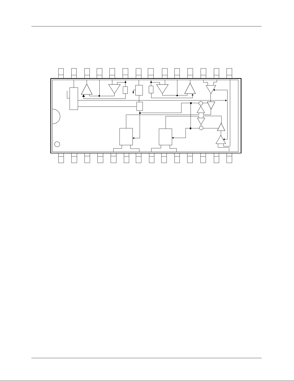
Internal Block Diagram
SGND
FGOUT
VCTL
H2P
FGIN
FG(V25)
VREG
FGAMPOUT
PG(V25)
PGAMPOUT
PGIN
1920212223242526
PGOUT
H2N
1428 27
161718
H1N
15
CTL
V
YS.
H
NC
COM
Control
NC
CTL
I
Current/Voltage
23
14
PVCC2
−
+
AMP
45 7 9
REF
REG
V
DRIVER
(5.0V)
V
Supply ea c h block
TSD
6
NC
OUT2P
PGND2
OUT2N
+
REF
V
8
OUT1P
AMP
-
HYS.
COM
DRIVER
10
11
NC
OUT1N
PGND1
+ -
±
AMP
GM
GM
±
12
PVCC1
13
+ -
SVCC
AMP
14
H1P
4
Rev. 1.0.1
February. 2000.

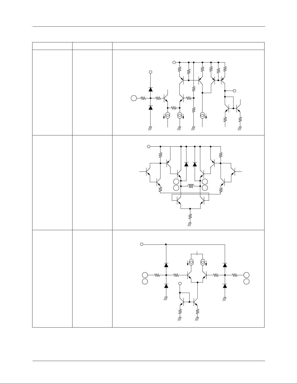
Equivalent Circuits
Description Pin No. Internal circuit
V
CTL
Motor output 5,7,8,10
27
V
REG
50
27
V
CC
1k
FAN8486D (KA3086D)
I
CTL
Hall input 14,15,16,17
V
REG
5
8
50
14
16
500
I
CTL
Vcc
7
10
500 50
15
17
Rev. 1.0.1
February. 2000.
5
 Loading...