

Fairchild Semiconductor FAN8423D3 Datasheet
FAN8423D3
3-Phase BLDC Motor Driver
www.fairchildsemi.com
Features
• 3-phase, full-wave, linear BLDC motor driver
• Power save at stop mode
• Built-in current limiter
• Built-in TSD (thermal shutdown) circuit
• Built-in 3X and 1X hall FG output
• Built-in hall bias circuit
• Built-in rotational direction detector
• Built-in reverse rotation preventer
• Built-in short braker
• Corresponds to 5 V DSP
Description
The FAN8423D3 is a monolithic IC, suitable for a 3-phase
spindle motor driver of a CD-media system.
28-SSOPH-375SG2
Typical Applications
• Compact disk ROM (CD-ROM) spindle motor
• Compact disk RW (CD-RW) spindle motor
• Digital video disk ROM (DVD-ROM) spindle motor
• Digital video disk RAM (DVD-RAM) spindle motor
• Digital video disk Player (DVDP) spindle motor
• Other compact disk media spindle motor
• Other 3-phase BLDC motor
©2000 Fairchild Semiconductor International
Ordering Information
Device Package Operating Temp.
FAN8423D3
FAN8423D3TF 28-SSOPH-375SG2
28-SSOPH-375SG2
−25°C ~ +75°C
−25°C ~ +75°C
Rev. 1.0.1
Oct. 2000.
FAN8423D3
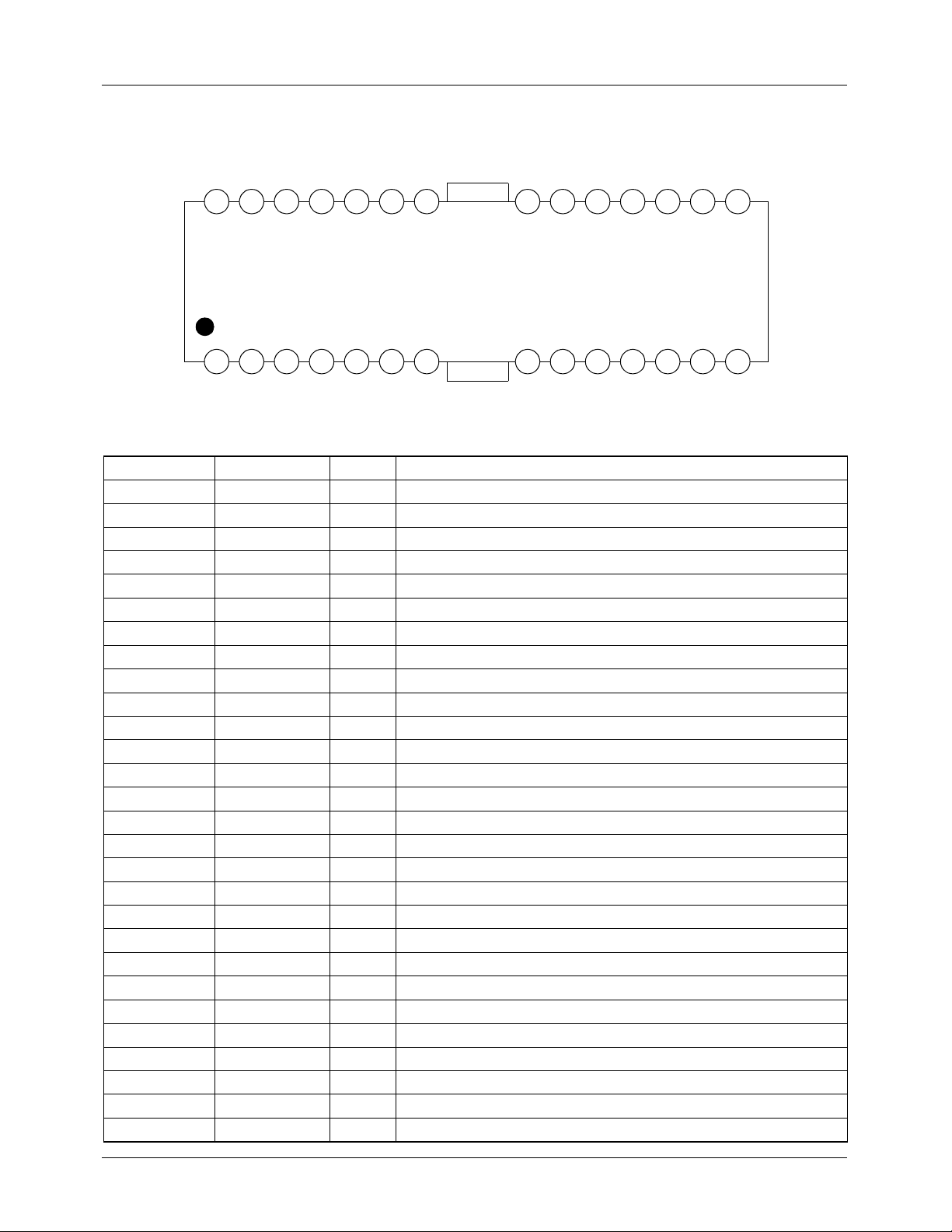
Pin Assignments
CS1
VM
NC
VCC
S/S
FG1X
EC
FIN(GND)
ECR
DIR
FG3X
SB
PC1
FAN8423D3
1 2 3 4 5 6 7 8 9 10 11 12 13 14
NC
A3
NC
A2
NC
NC
A1
FIN(GND)
GND
H1+
H1-
H2+
H2-
Pin Definitions
Pine Number Pin Name I/O Pin Function Description
1 NC - No connection
2 A3 O Output (A3)
3 NC - No connection
4 A2 O Output (A2)
5 NC - No connection
6 NC - No connection
7 A1 O Output (A1)
8 GND - Ground
9 H1+ I Hall signal (H1+)
10 H1- I Hall signal (H1-)
11 H2+ I Hall signal (H2+)
12 H2- I Hall signal (H2-)
13 H3+ I Hall signal (H3+)
14 H3- I Hall signal (H3-)
15 VH I Hall bias
16 NC - No connection
17 PC1 - Phase compensation capacitor
18 SB I Short brake
19 FG3X O FG waveform (3X)
20 DIR O Rotational direction output
21 ECR I Output current control reference
22 EC I Output current control voltage
23 S/S I Power save (Start/Stop switch)
24 FG1X O FG waveform (1X)
25 VCC - Supply voltage (Signal)
26 NC - No connection
27 VM - Supply voltage (Motor)
28 CS1 - Output current detection
NC
H3+
VH
1516171819202122232425262728
H3-
2
Rev. 1.0.1
Oct. 2000.
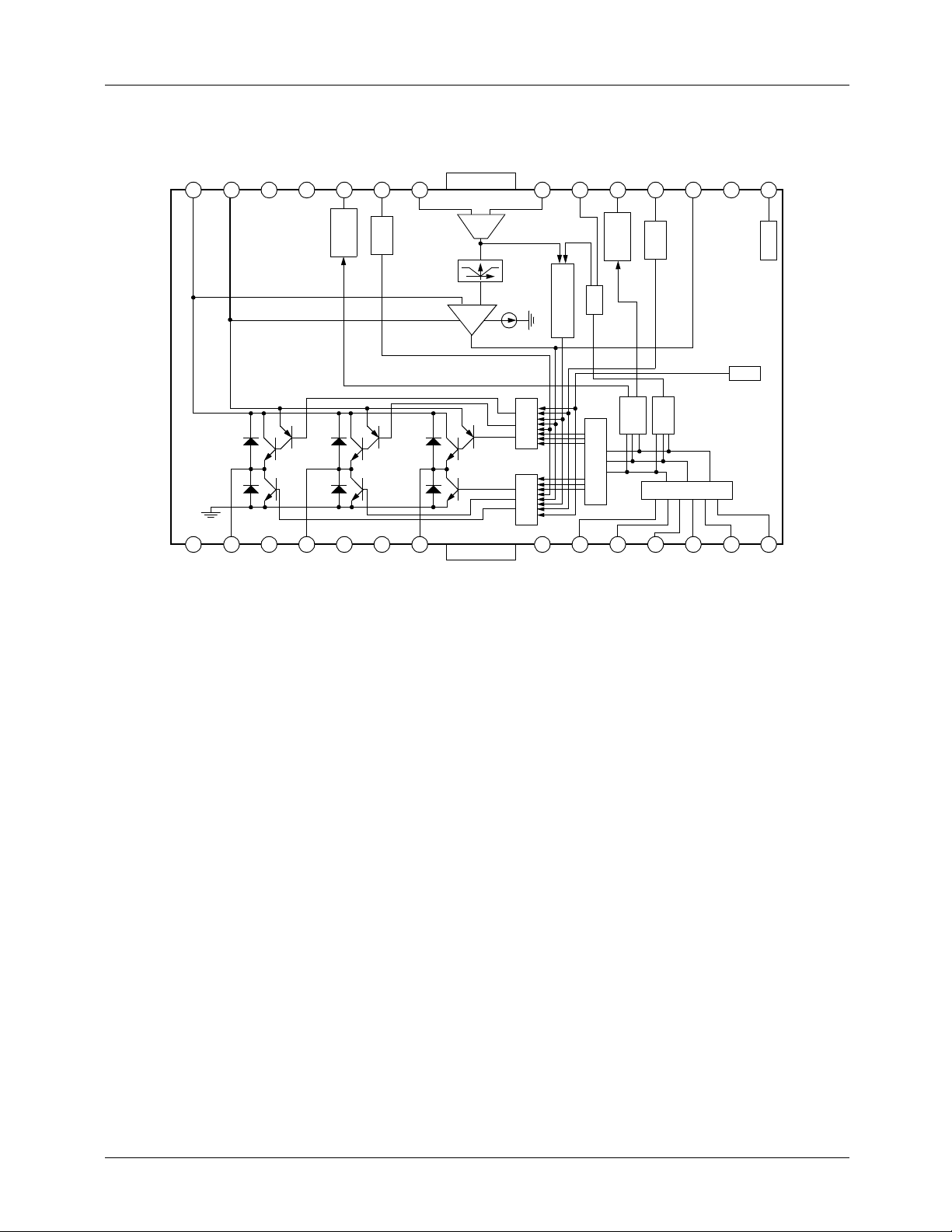
Internal Block Diagram
CS1
VM
NC
28 27 26 25 24 23 22 21 20 19 18 17 16 15
VCC
FG1X
FG1X
Generator
S/S
Stop
Start
EC
Current Sense
Amp
GND
-
+
Output
Current Limit
Absolute
Values
Upper
Lower
Distribu-
Distribu-
FAN8423D3
ECR
DIR
FG3X
SB
PC1
NC
VH
Short
FG3X
tion
Logic
Brake
Generator
Reverse Rota-
tor
tion
Direc-
Detec-
Selector
Commutation
Hall Amp
Hall
TSD
1234567
NC
A3
NC
A2
NC
NC
A1
GND
8
91011121314
GND
H1-
H1+
H2-
H2+
H3-
H3+
Rev. 1.0.1
Oct. 2000.
3
FAN8423D3
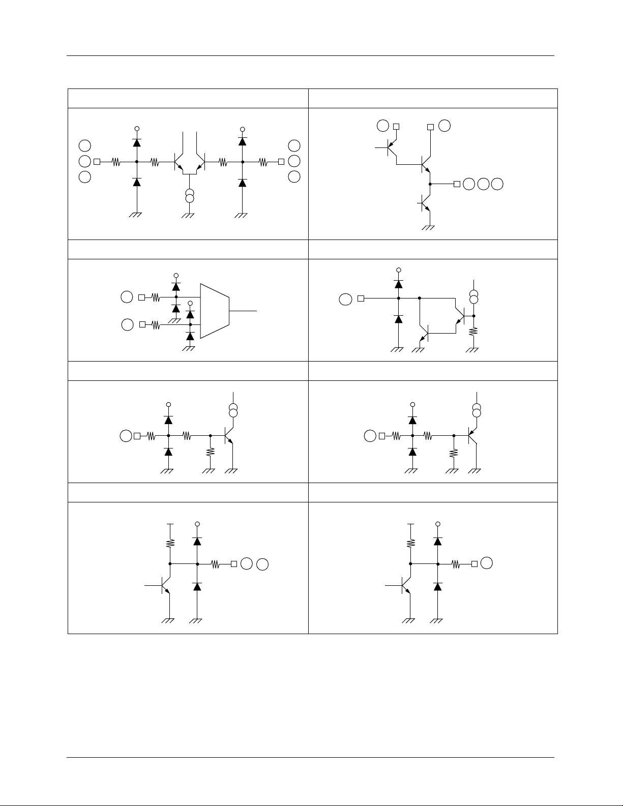
Equivalent Circuits
Hall Input Driver Output
28
9
50Ω
11
13
1KΩ
1KΩ
50Ω
10
12
14
2274 7
Torque Control Input Hall Bias Input
50Ω
21
50Ω
22
+
-
15
100KΩ
Start/stop Input Short Brake Input
50Ω
23
40KΩ
30KΩ
50Ω
18
1KΩ
20KΩ
Fg Output Dir Output
Vcc
10KΩ
50Ω
4
19
24
Rev. 1.0.1
Oct. 2000.
30KΩ
Vcc
50Ω
20
Absolute Maximum Ratings (Ta = 25°°°°C)
Parameter Symbol Value Unit
Maximum supply voltage (Signal) V
Maximum supply voltage (Motor) V
Power dissipation P
Maximum output current I
Operating temperature range T
Storage temperature range T
NOTE:
1. When mounted on a 76 .2mm × 114mm × 1.57mm PCB (Phenolic resin material).
2. Power dissipation reduces 16.6mW/°C for using above Ta = 25°C
3. Do not exceed P
and SOA (Safe operating area).
D
CCmax
Mmax
D
Omax
OPR
STG
7V
15 V
note
2.5
1.3 A
-25 ~ +75 °C
-55 ~ +150 °C
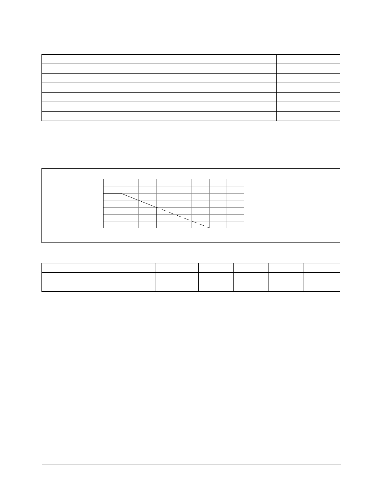
Power Dissipation Curve
Pd (mW)
3,000
2,000
FAN8423D3
W
1,000
SOA
0
0 25 50 75 100 125 150 175
Recommended Operating Conditions (Ta = 25°°°°C)
Parameter Symbol Min. Typ. Max. Unit
Supply Voltage V
Motor Supply Voltage V
cc
M
4.5 5 5.5 V
3.5 12 14 V
Ambient temperature, Ta [°C]
Rev. 1.0.1
Oct. 2000.
5

FAN8423D3
Electrical Characteristics
(Unless otherwise specified, Ta = 25 °C, Vcc=5 V, VM=12 V)
Parameter Symbol Condition Min. Typ. Max. Unit
Quiescent circuit current 1 I
Quiescent circuit current 2 I
cc1
cc2
START/STOP
On voltage range V
Off voltage range V
SSon
SSoff
HALL BIAS
Hall bias voltage V
HB
HALL AMP
Hall bias current I
Common-mode input range V
Minimum input level V
H1 hysteresis level V
HA
HAR
INH
HYS
TORQUE CONTROL
Ecr Input voltage range E
Ec Input voltage range E
Offset voltage (-) E
Offset voltage (+) E
Ec Input current E
Ecr Input current E
Input/output gain G
CR
C
Coff-
Coff+
Cin
CRin
EC
FG
FG output voltage (H) V
FG output voltage (L) V
FGh
FGl
Duty (reference value) - - - 50 - %
OUTPUT BLOCK
Saturation voltage (upper TR) V
Saturation voltage (lower TR) V
Torque limit current I
OH
OL
TL
DIRECTION DETECTOR
DIR output voltage (H) V
DIR output voltage (L) V
DIRh
DIRl
SHORT BRAKE
ON voltage range V
OFF voltage range V
SBon
SBoff
At stop mode - - 0.2 mA
At start mode - 5 10 mA
Output driver ON 2.5 - Vcc V
Output driver OFF 0.0 - 1.0 V
IHB=20 mA 0.4 1.0 1.8 V
--0.52µA
- 1.0 - 4.0 V
-60--mVpp
- 5 20 40 mVpp
- 1.0 - 4.0 V
- 1.0 - 4.0 V
Ec=2.5 V -80 -50 -20 mV
Ec=2.5 V 20 50 80 mV
Ec=2.5 V - 0.3 3 µA
Ecr=2.5 V - 0.3 3 µA
Ec=2.5 V, Rcs=0.5 Ω 0.41 0.51 0.61 A / V
Ifg=-10 µA4.54.9-V
Ifg=10 µA--0.5V
Io=-300 mA - 0.9 1.4 V
Io=300 mA - 0.4 0.7 V
RCS=0.5 Ω 560 700 840 mA
IFG=-10 µA4.54.7-V
IFG=10 µA--0.5V
-2.5-VccV
-0-1.0V
6
Rev. 1.0.1
Oct. 2000.
 Loading...