

Fairchild Semiconductor FAN8400BD3 Datasheet

©2001 Fairchild Semiconductor Corporation
www.fairchildsemi.com
Rev.1.0.1
Features
• 3-Phase BLDC motor driver IC with speed control
• Phase Locked Loop (PLL) speed control
• Built-in phase locked detector output
• Current linear drive scheme
• External clock for arbitrary motor speed
• Built-in FG amplifier and integrating amplifier
• Auto Gain Control (AGC) circui t for compensation hall
amplifier
• Built-in protection circuits (over-current limit, under
voltage limit, thermal shut down)
Description
The FAN8400D is a monolithic integrated circuit. it is one
driver for laser beam printe r (LBP) polygon mirror motor,
which has single chip implementation of all circuits. For
extremely high rotational precision, it employs the phase
locked loop (PLL) speed control scheme.
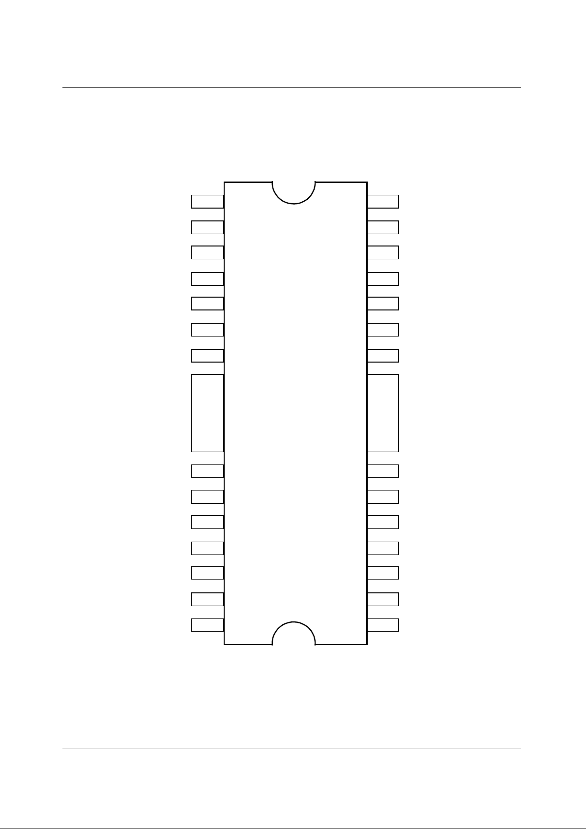
28-SSOPH-375SG2
Typical application
• Polygon mirror motor drive IC for laser beam printer
• Polygon mirror motor drive IC for facsimile
• Polygon mirror motor drive IC for duplicator
• Polygon mirror motor driv e IC for multi function printer
• General 3 phase BLDC motor drive IC
Ordering Information
Device Package Operating Temp
FAN8400BD3 28-SSOPH-375SG2 −20°C ~ +80°C
FAN8400BD3TF 28-SSOPH-375SG2 −20°C ~ +80°C
FAN8400D (FAN8400BD3)
3-Phase BLDC Motor Driver with PLL
FAN8400D (FAN8400BD3)
2
Pin Assignments
AGC
FIN
1
2
3
4
5
6
7
8
9
10
11
12
13
14
FIN
28
27
26
25
24
23
22
21
20
19
18
17
16
15
FG
IN-
FG
S
FG
OUT
S/S
NC
SGND
LD
ECLK
PD
E
I
E
O
F
C
NC
V
REG
V
CC
PGND
R
F
U
V
W
H
V+
H
V-
H
U+
H
U-
H
W+
H
W-
FAN8400D
NC

FAN8400D (FAN8400BD3)
3
Pin Definitions
Pin Number Pin Name Pin Function Description
1 AGC AGC amplifier frequency characteristics correction
2FG
IN-
FG amplifier inverting input
3FG
S
FG pulse output
4FG
OUT
FG amplifier output
5 S/S Stop and start
6NC 7NC 8 SGND Signal ground
9 LD Phase locked loop detector output
10 ECLK External clock
11 PD Phase locked loop detector output
12 E
I
Error amplifier inverting input
13 E
O
Error amplifier output
14 F
C
Control amplifier frequency correction
15 NC 16 V
REG
Regulator voltage stabilization output
17 V
CC
Power supply
18 PGND Power ground
19 R
F
Output current detection
20 U U output
21 V V output
22 W W output
23 H
V+
V hall amplifier non inverting input
24 H
V-
V hall amplifier inverting input
25 H
U+
U hall amplifier non inverting input
26 H
U-
U hall amplifier inverting input
27 H
W+
W hall amplifier non inverting input
28 H
W-
W hall amplifier inverting input

FAN8400D (FAN8400BD3)
4
Internal Block Diagram
AGC
FIN
1
2
3
4
5
6
7
8
9
10
11
12
13
14
FIN
28
27
26
25
24
23
22
21
20
19
18
17
16
15
FG
IN-
FG
S
FG
OUT
S/S
NC
SGND
LD
ECLK
PD
E
I
E
O
F
C
NC
V
REG
V
CC
PGND
R
F
U
V
W
H
V+
H
V-
H
U+
H
U-
H
W+
H
W-
V
REG
2
V
REG
2
Regulator
Output
Controller
Hall
AMP
Matrix
AGC
Clock
PLL
Lock
Detector
TSD &
UVLO
-
+
S/S
-
+
-
+
OCL
V-type
Control
NC

FAN8400D (FAN8400BD3)
5
Absolute Maximum Ratings (Ta = 25°°°°C)
Recommended Operating Conditions (Ta = 25°°°°C)
Parameter Symbol Value Unit Remark
Maximum supply voltage V
CCMAX
30 V -
Maximum output current I
OMAX
0.6 A Power dissipation Pd 1.7 W Operating temperature T
OPR
−20 ~ +80 °C-
Storage temperature T
STG
−50 ~ +150 °C-
Parameter Symbol Min. Typ. Max. Unit
Operating voltage range V
CC
20 24 28 V
 Loading...