

Fairchild Semiconductor FAN8200D, FAN8200 Datasheet

www.fairchildsemi.com
FAN8200/FAN8200D/FAN8200MTC
FAN8200MP
Low Voltage/Low Saturation Stepping Motor Driver
Features
• 3.3V and 5V MPU interface
• Dual H-bridge drivers for bipolar stepping motor drives
• Built-in vertical-PNP power transistors
• Wide supply voltage range (V
• Low saturation voltage (0.4V@ 0.4A)
• Built-in chip enable function for each bridge
• Built-in shoot-through current protection
• Built-in thermal shutdown(TSD) function
= 2.5V ~ 7.0V)
CC
Description
The FAN8200/FAN8200D/FAN8200MTC/FAN8200MP is a
monolithic intergrated circuit designed for two-phase stepping motor drive systems. It has dual H-bridge drivers with
vertical-PNP power transistors. Each of the bridges has an
independant enable pin, therefore it can be used for other
applications as well as stepping motor drive systems.
14-DIP-300
1
14-SOP-225
1
14-TSSOP
1
14-MLP
Typical Application
• General low voltage stepping motor driver
• Floppy disk driver
• Camera stepping motor driver
• PC camera or security equipment motion controller
• Two channel DC motor driver for a digital still camera
(DSC)
• MPU interfaced general power driver (buffer)
©2003 Fairchild Semiconductor Corporation
Ordering Information
Device Package Operating Temp.
FAN8200 14-DIP-300 -20 ~ +75°C
FAN8200D 14-SOP-225 -20 ~ +75°C
FAN8200DTF 14-SOP-225 -20 ~ +75°C
FAN8200MTC 14-TSSOP -20 ~ +75°C
FAN8200MTCX 14-TSSOP -20 ~ +75°C
FAN8200MP
FAN8200MPX
14-MLP -30 ~ +80°C
Rev. 1.0.4

FAN8200/FAN8200D/FAN8200MTC FAN8200MP
Pin Assignments
PGND
CE2
OUT3
VS2
OUT4
1011121314
IN2
PGND
98
FAN8200/FAN8200D/
8200MTC/8200MP
1234567
V
CC
CE1
OUT1
VS1
OUT2
IN1
SGND
Pin Definitions
Pin Number Pin Name I/O Pin Function Description
1V
CC
2 CE1 I Chip enable 1
3 OUT1 O Output 1
4 VS1 - Power supply 1
5 OUT2 O Output 2
6 IN1 I Input 1
7 SGND - Signal ground
8 PGND - Power ground
9 IN2 I Input 2
10 OUT4 O Output 4
11 VS2 - Power supply 2
12 OUT3 O Output 3
13 CE2 I Chip enable 2
14 PGND - Power ground
- Logic part supply voltage
2

Internal Block Diagram
V
1
CC
FAN8200/FAN8200D/FAN8200MTC FAN8200MP
4
VS1
3
OUT1
IN1
CE1
SGND
IN2
CE2
50K
6
80K
50K
2
80K
7
50K
9
80K
50K
13
80K
Control
Part1
Control
Part2
TSD &
BIAS
5
OUT2
8
PGND
11
VS2
12
OUT3
10
OUT4
14
PGND
3
FAN8200/FAN8200D/FAN8200MTC FAN8200MP
Absolute Maximum Ratings (Ta = 25°C)
Parameter Symbol Value Unit
Supply voltage V
Power supply voltage V
Output voltage V
Input voltage V
Peak output current per channel I
Continuous output current per channel I
Power dissipation P
Junction temperture T
Storage temperature T
Operating temperature T
Notes:
1. When mounted on 76.2mm
2. Power dissipation reduces 8.0mW/
FAN8200MP for Ta ≥ 25°C.
3. Should not exceed P
× 114mm × 1.57mm PCB (glass epoxy material).
°C for FAN8200, 4.8mW/°C for FAN8200D, 6.9mW/°C for FAN8200MTC and 6.4mW/°C
and SOA(Safe Operating Area).
D
CC(MAX)
S(MAX)
OUT(MAX)
IN(MAX)
O(PEAK)
O
note
D
J
STG
A
0.65 (FAN8200)
0.4 (FAN8200D)
0.55 (FAN8200MTC)
0.35 (FAN8200MP)
1.0 (FAN8200)
0.6 (FAN8200D)
0.87 (FAN8200MTC)
0.8 (FAN8200MP)
-20 ~ 75(FAN8200)
-20 ~ 75(FAN8200D)
-20 ~ 75(FAN8200MTC)
-30 ~ 80(FAN8200MP)
9.0 V
9.0 V
VS + V
CF
7.0 V
1A
150 °C
-40 ~ 125 °C
V
A
W
°C
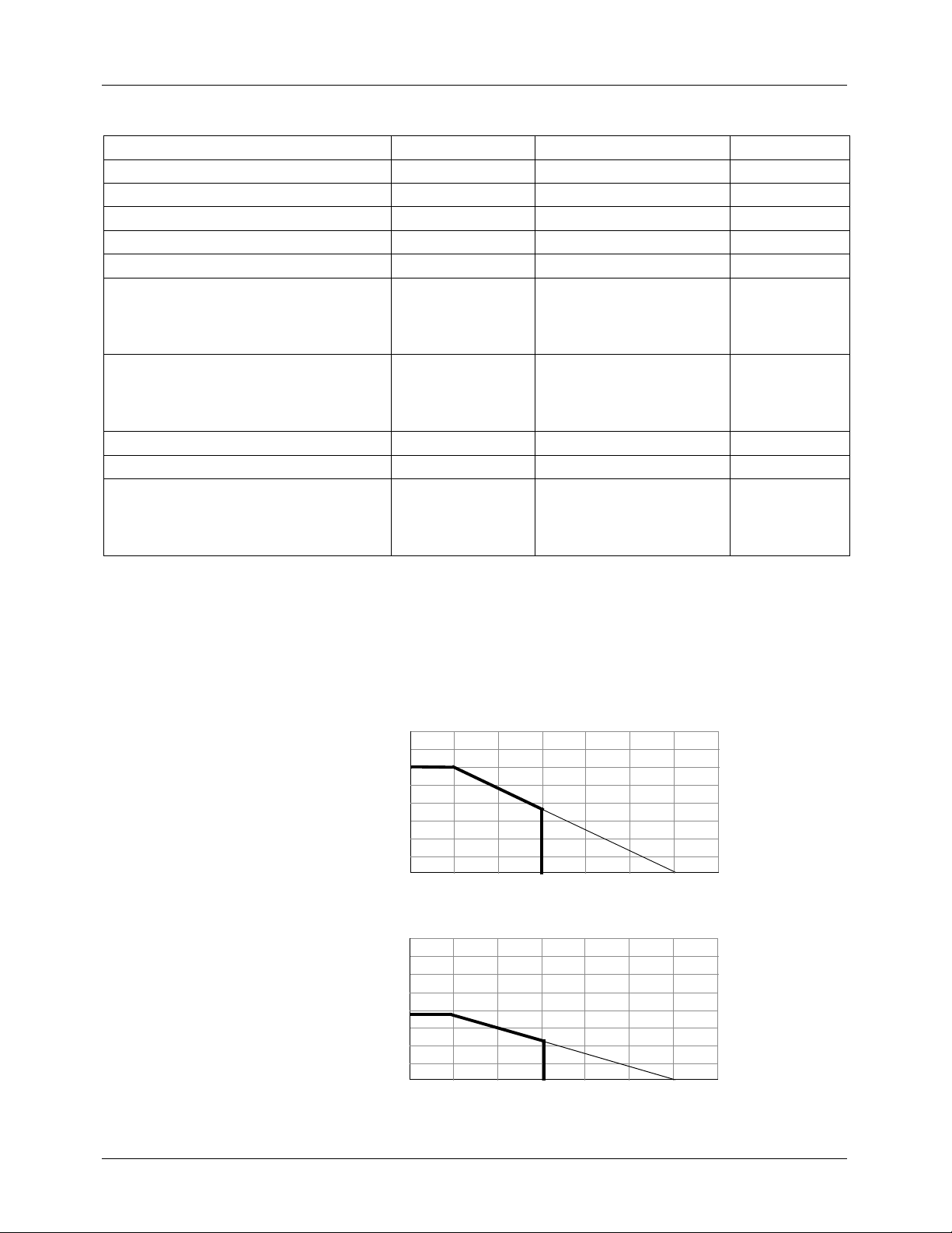
Power Dissipation Curve
Power
Dissipation
FAN8200
FAN8200D
: PD[W]
Power
Dissipation
: PD[W]
1.0
0.5
1.0
0.6
SOA
0
0255075100125
Ambient temperature, Ta [°C]
SOA
0
0255075100125
Ambient temperature, Ta [°C]
150 175
150 175
4
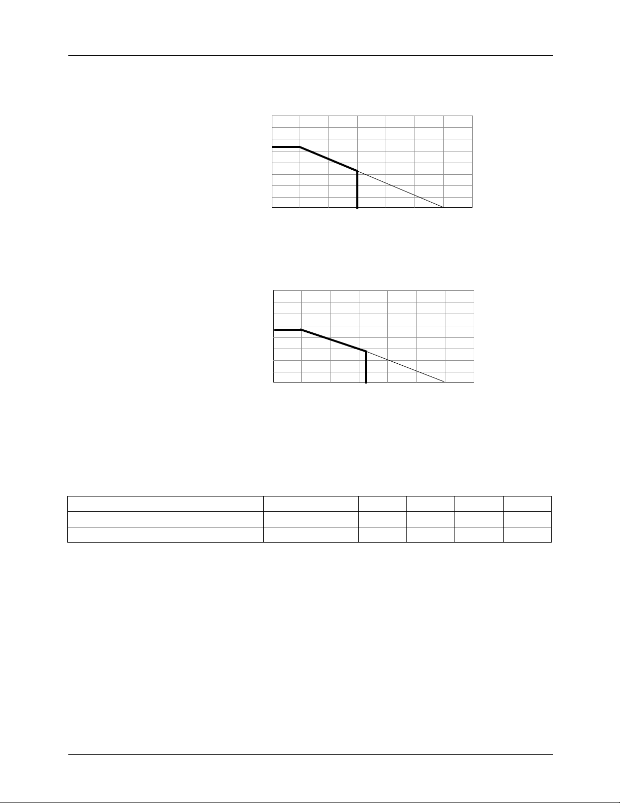
Power Dissipation Curve (Continued)
FAN8200/FAN8200D/FAN8200MTC FAN8200MP
FAN8200MTC
FAN8200MP
Power
Dissipation
: PD[W]
Power
Dissipation
: PD[W]
1.0
0.5
1.0
0.5
SOA
0
0255075100125
Ambient temperature, Ta [°C]
SOA
0
0255075100125
Ambient temperature, Ta [°C]
150 175
150 175
Recommended Operating Conditions (Ta = 25°C)
Parameter Symbol Min. Typ. Max Unit
Logic circuit supply voltage V
Power supply voltage V
CC
S
2.5 - 7.0 V
2.5 - 7.0 V
5
 Loading...